
Preparation and Characterization of Gallium Magnesium Zinc Oxide Transparent Conductive Thin Films
2018-12-29 00:52:04,,,
, , ,
(1 Experimental Teaching and Laboratory Management Center, South-Central University for Nationalities, Wuhan 430074, China; 2 College of Electronic Information Engineering, South-Central University for Nationalities, Wuhan 430074, China)
Abstract Gallium magnesium zinc oxide (GaMgZnO) transparent conductive thin films were prepared by magnetron sputtering method. The influence of deposition temperature on the structural and electro-optical properties of the thin films was studied by X-ray diffraction (XRD), four-point probe and ultraviolet-visible spectrometer. The results show that all the thin films are polycrystalline with a hexagonal structure and have a preferred orientation along the c-axis perpendicular to the substrate. The deposition temperature significantly affects the crystal quality and electro-optical properties of thin films. When the deposition temperature is at 550 K, the GaMgZnO thin film has the best crystalline quality and electro-optical properties, with the maximum grain size (51.72 nm), the minimum lattice strain (1.1110-3), the lowest dislocation density (3.73×10¹⁴ linem-2) and resistivity (1.63×10⁻³cm), and the highest average visible transmittance(82.41%) and figure of merit (5.06×10² -1cm-1). Furthermore, the optical energy gap of the deposited films were determined and observed to be larger than that of undoped ZnO due to Moss-Burstein effect.
Keywords magnetron sputtering; doped zinc oxide; transparent conductive thin film
Zinc oxide (ZnO) is an Ⅵ group semiconductor material with wide direct energy gap and wurtzite structure. The high stability, melting point and excitation energy make it a promising ultraviolet and blue optoelectronic material. In addition, ZnO semiconductor thin films have a wide range of applications in a variety of optoelectronics devices such as flat panel displays[1,2], solar cells[3,4], light-emitting diodes[5,6], thin film transistors[7]and chemical sensors[8-10]. A transparent conductive electrode is a necessary component of solar cells. Usually, it consists of a transparent conducting film (TCF) and a glass substrate. The most important commercial material for TCFs nowadays is indium-tin oxide (ITO), owing to its unique characteristics of high visible transmittance, low resistivity, high infrared reflectance and absorbance in the microwave region[11,12]. However, ITO is likely to become unavailable because the fast-growing semiconductor industries are faced with the limitation of indium resources and toxicity in the atmosphere[13,14]. In view of the depletion of ITO, the doped ZnO will be emerging as an alternative transparent electrode. Recently, much attention has been paid to the codoping process in which the two elements are doped into ZnO simultaneously, because the codoped ZnO thin films are expected to show some improvements in electrical and optical performance of TCFs. Up to now, the vanadium-aluminum[15], aluminum-indium[16], gallium-indium[17], aluminum-gallium[18], boron-gallium[19], magnesium-aluminum[20], aluminum-titanium[21]and gallium-titanium[22]codoping cases have been reported. As is known, although many experimental studies have been conducted on the synthesis and electrical properties of the codoped ZnO thin films, there are few quantitative studies on their electro-optical properties. In this study, the gallium magnesium zinc oxide (GaMgZnO) transparent conductive thin films were prepared on glass substrates by magnetron sputtering technique. The influence of deposition temperature on the microstructure, electrical and optical properties of the thin films was investigated by X-ray diffraction (XRD), four-probe meter and ultraviolet-visible spectrometer.
1 Experiment
TheGaMgZnO samples were deposited on the clean glass substrates by using radio frequency magnetron sputtering technique. A sintered GaMgZnO ceramic sputter target (2 wt% Ga2O3: 2 wt% MgO : 96 wt% ZnO, 99.99% purity) was employed as source material. The sputtering chamber was evacuated to a base pressure below 3.1×10⁻⁴Pa before argon gas. After vacuum pumping, the sputtering argon gas with a purity of 99.999% was introduced into the chamber and controlled by the standard mass flow controllers. Before deposition of the GaMgZnO samples, pre-sputtering was conducted for about 10 min to attain stability and to remove impurities. The deposition parameters for preparing GaMgZnO samples were as follows: the substrate-target distance, 75 mm; the sputtering power, 130 W; operating pressure, 3 Pa; and sputtering time, 45 min. In order to investigate the influence of deposition temperature on properties of the GaMgZnO thin films, the deposition temperature was changed from 350 to 650 K. The thickness of the samples was measured by a surface profiler (Alpha-step 500). X-ray diffraction studies were conducted to determine the crystal structure with a D8-Advance diffractometer using Cu Kradiation at 40 kV and 40 mA. The electrical properties were evaluated using a four-point probe measurement system (RH-2035). Optical properties of the films were examined with the normal incident transmittance measured by a double-beam spectrometer (TU-1901). All measurements were performed at room temperature in ambient air.
2 Results and discussion
2.1 Structural properties of the thin films
Fig.1 shows the XRD patterns of GaMgZnO samples prepared at different deposition temperatures. These XRD peaks are assigned to ZnO according to the Joint Committee of Powder Diffraction Standards Card (JCPDS 36-1451). Note that all the samples exhibit a dominant (002) peak with slight (004) peak in the displayed 2θregion, which indicates that the GaMgZnO thin films have highly preferred orientation with their crystallographicc-axis perpendicular to the substrates, irrespective of deposition temperature. Note also that neither metallic Ga or Mg characteristic peaks nor Ga2O3or MgO peaks was observed from the XRD patterns, which implies that the dopants have not destroyed the ZnO structure and act as typical dopants. Corresponding to the deposition temperatures of 450, 550 and 650 K, the intensity ratio of (004) to (002) (I(004)/I(002)) and the intensity of (002) peak (I(002)) for the samples are found from Fig.2 to be 2.14%, 2.59104cps; 1.96%, 4.63104cps; and 2.11%, 2.98104cps, respectively. As is obvious, the values ofI(004)/I(002)andI(002)are observed to rise initially and then fall with the increase of deposition temperature. The GaMgZnO sample prepared at 550 K has the minimumI(004)/I(002)and the maximumI(002).

Fig.1 The XRD patterns of GaMgZnO samples prepared at deposition temperature of (a) 450 K,(b) 550 K and (c) 650 K, respectively圖1 溫度為(a) 450 K, (b) 550 K和(c) 650 K時(shí)GaMgZnO樣品的XRD圖譜

Fig.2 Effect of deposition temperature on I(002) and I(004)/I(002) of GaMgZnO samples圖2 沉積溫度對(duì)GaMgZnO樣品I(002)和I(004)/I(002)的影響
The grain size of the deposited samples was calculated from the diffraction peaks of (002) plane using the Scherrer’s formula[23,24]:
(1)
(2)
(3)
The values ofB,D,andof all the deposited samples are presented in Fig.3 and Fig.4, respectively. With the increment of deposition temperature, theB,andrise in advance and then fall, but theDtakes on an opposite trend. When the deposition temperature is 550 K, the deposited GaMgZnO sample exhibits the best crystalline and microstructural properties, with the narrowestBof 2.77×10⁻³rad, the largestDof 51.72 nm, the minimumof 3.73×10¹⁴linem-2and the lowestof 1.11×10⁻³. The results suggest that the crystal quality of the GaMgZnO thin films is strongly dependent upon the deposition temperature.
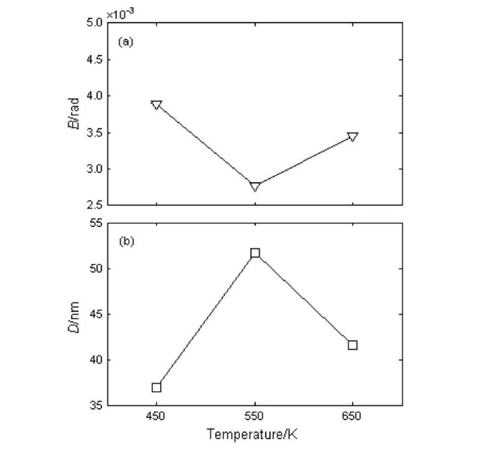
Fig.3 Effect of deposition temperature on B and D of GaMgZnO samples圖3 沉積溫度對(duì)GaMgZnO樣品B和D的影響

Fig.4 Effect of deposition temperature on and of GaMgZnO samples圖4 沉積溫度對(duì)GaMgZnO樣品 和 的影響
2.2 Electrical and optical properties of the thin films
Fig.5 presents the variation of the resistivity () with deposition temperature for the GaMgZnO samples. As the deposition temperature from 450 to 550 K, thefalls firstly and then rises. The minimumof 1.63×10⁻³cm is obtained at the deposition temperature of 550 K. The decrease of resistivity can be attributed to the improvement of crystalline quality and the increase of carrier concentration.
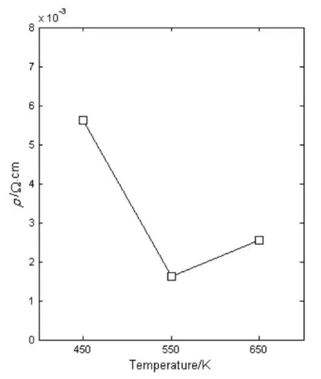
Fig.5 Shows of deposition temperature on of GaMgZnO samples圖5 沉積溫度對(duì)GaMgZnO樣品 的影響
Fig.6 gives the optical transmittance (T) curves of GaMgZnO samples with glass substrates prepared at different deposition temperatures. All the transmission spectra show interference pattern with sharp fall of transmittance at the band edge, which is an indication of good crystallinity. Fig.7(a) shows the variation of the average visible transmittance (Tav) with deposition temperature for the GaMgZnO samples. As can be seen, the average transmittance in the visible range (Tav) increases slightly with the deposition temperature rising up to 550 K, and then significantly decreases when the deposition temperature is over 550 K. The highestTavof 82.41% for the GaMgZnO thin film with glass substrate can be achieved at the deposition temperature of 550 K. This enhancement in the optical transmittance is closely related to the improvement of crystallinity and the increase of grain size of the deposited films.

Fig.6 The transmittance curves of GaMgZnO samples prepared at deposition temperature of (a) 450 K, (b) 550 K and (c) 650 K, respectively圖6 沉積溫度為(a) 450 K, (b) 550 K和(c) 650 K時(shí)GaMgZnO樣品的透過率曲線圖

Fig.7 Effect of deposition temperature on Tav and FTC of GaMgZnO samples圖7 沉積溫度對(duì)GaMgZnO樣品Tav和FTC的影響
In order to quantify the electro-optical properties of the deposited films, the figure of merit (FTC) is given by the formula[27,28]:
(4)
whereTavis the average visible transmittance andis the resistivity of the films. Fig.7(b) displays the variation ofFTCwith deposition temperature for the deposited samples. As the deposition temperature increases, theFTCfirst increases and then decreases and reaches its maximum value of 5.06×10²-1cm-1at the deposition temperature of 550 K. The increase inFTCwith deposition temperature was due to increase inTavand decrease in. It is known that the higher theFTC, the better quality of the transparent conductive film. Thus, in this study, it can be concluded that the optimum deposition temperature is 550 K.
2.3 Optical energy gap of the thin films
According to the solid band theory, the direct optical energy gap (Eg) of the deposited films can be determined by the following equations[29,30]:
(αE)m=B(E-Eg),
(5)
(6)
whereBis a constant,is the absorption coefficient,Eis the photon energy,his the Planck constant,cis the light velocity,is the wavelength of incident light andmis 2 for direct energy gap semiconductors. Fig.8 presents the Tauc plots of (E)2-Efor GaMgZnO samples prepared at different deposition temperatures. The linear dependence of (E)2onEat higher photon energies indicates that the GaMgZnO thin films are essentially direct-transition-type semiconductors. TheEgvalues were obtained by extrapolation method[31-33]and plotted in Fig.9. The optical energy gaps of GaMgZnO thin films are found to be ranging from 3.362 to 3.531 eV, larger than that of pure ZnO. The widening of optical energy gap may be attributed to Moss-Burstein effect. This effect is due to the fact that the conduction band filling in highly degenerate semiconductor makes the Fermi level exceed the conduction band minimum. Similar results have been reported in the previously literature[34-36].

Fig.8 Tauc plots for GaMgZnO samples prepared at deposition temperature of (a) 450 K, (b) 550 K and (c) 650 K, respectively圖8 沉積溫度為(a) 450 K, (b) 550 K和(c) 650 K時(shí)GaMgZnO樣品的Tauc圖

Fig.9 Effect of deposition temperature on Eg of GaMgZnO samples圖9 沉積溫度對(duì)GaMgZnO樣品Eg的影響
3 Conclusion
In this work, the transparent conducting GaMgZnO thin films were prepared by magnetron sputtering technique, and the influence of the deposition temperature on the structural, electrical and optical properties was investigated. It is found that all the deposited films have hexagonal wurtzite structure with highlyc-axis orientation. The GaMgZnO thin film prepared at the deposition temperature of 550 K possesses the best crystallinity and electro-optical properties, which have the maximum grain size (51.72 nm), the minimum lattice strain (1.11×10⁻³), the lowest dislocation density (3.73×10¹⁴linem-2) and the highest figure of merit (5.06×10²-1cm-1). The optical energy gaps of the thin films were determined and observed to be larger than that of undoped ZnO due to Moss-Burstein effect. The results demonstrate that the crystal quality, electrical and optical properties of the GaMgZnO thin films are closely related to the deposition temperature.
猜你喜歡
礦山安全信息(2021年21期)2021-07-04 06:33:32
少先隊(duì)活動(dòng)(2020年12期)2021-01-14 01:47:40
礦山安全信息(2020年37期)2020-12-26 07:25:58
礦山安全信息(2020年2期)2020-03-05 05:13:56
礦山安全信息(2020年3期)2020-03-04 10:18:08
沉積與特提斯地質(zhì)(2019年1期)2019-07-16 08:41:30
沉積與特提斯地質(zhì)(2018年4期)2018-07-16 08:27:30
中成藥(2017年3期)2017-05-17 06:09:01
南方文學(xué)(2016年4期)2016-06-12 19:58:50
領(lǐng)導(dǎo)科學(xué)論壇(2016年9期)2016-06-05 14:59:58
