
Impact of symmetric gate-recess length on the DC and RF characteristics of InP HEMTs
2022-01-23 06:35:18RuizeFeng封瑞澤BoWang王博ShuruiCao曹書睿TongLiu劉桐YongboSu蘇永波
Chinese Physics B 2022年1期
Ruize Feng(封瑞澤) Bo Wang(王博) Shurui Cao(曹書睿) Tong Liu(劉桐) Yongbo Su(蘇永波)
Wuchang Ding(丁武昌)1,2, Peng Ding(丁芃)1,2,?, and Zhi Jin(金智)1,2,?
1High-Frequency High-Voltage Device and Integrated Circuits Center,Institute of Microelectronics,Chinese Academy of Sciences,Beijing 100029,China
2University of Chinese Academy of Sciences,Beijing 100029,China
3Guangxi Key Laboratory of Precision Navigation Technology and Application,Guilin University of Electronic Technology,Guilin 541004,China
Keywords: InP HEMT,InGaAs/InAlAs,current gain cut-off frequency(fT),maximum oscillation frequency(fmax),gate-recess length(Lrecess)
1. Introduction
TheLSDis composed of the cap layer length(Lcapped)and the gate-recess length(Lrecess).Therefore,the change ofLSDis essentially a compromise between the cap layer length and the gate-recess length(Lrecess).Takahashiet al.[8]reported that thefmaximproved significantly by extending the drain-side gaterecess length (LRD) to 250 nm; meanwhile, the source-side gate-recess length(LRS)was kept to 70 nm;Shinoharaet al.[9]reported that the asymmetric recess technique is one of the effective solutions to achieve a higherfmaxsince a longerLRDresults in much reducedgdandCgd/Cgs. Kimet al.[10]reported that they improved short-channel effects through widening of the side-recess spacing (Lside) to 150 nm, as well as reducing parasitic source and drain resistances. Shinoharaet al.[11]reported that thefTdecreases with increasingLRS. This variation can be explained by the increase in the source resistance(RS)due to the spread of the highly resistive recessed region.In these reports, it is confirmed that the variation of the gaterecess length (Lrecess) has a significant impact on the characteristics of the devices. On this basis,we want to further study the impact of changing the gate-recess length (Lrecess) on the performance of the devices when theLSDremains unchanged.
In this work,we fabricated a set of symmetric gate-recess devices with gate length of 70 nm while maintaining the length of source-drain metal and gate length(Lg)constant. By controlling theLSDunchanged, we study the impact of different symmetric gate-recess length(Lrecess)on the DC and RF performance of the devices.
2. Experiment
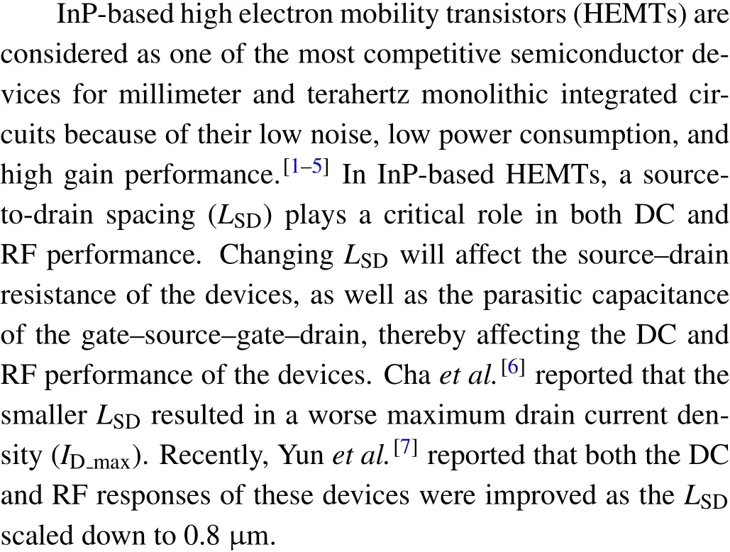
The schematic illustration of the cross-section of the InPbased HEMTs is shown in the following Fig. 1. The epitaxial layers of the devices were grown by gas source molecular beam epitaxy (GSMBE) on 3-inch (1 inch = 2.54 cm)semi-insulating InP(100)substrates. From bottom to top,the layers consist of a 500-nm In0.52Al0.48As buffer layer,10-nm ln0.53Ga0.47As channel layer, 3-nm unstrained ln0.52Al0.48As spacer layer, Si delta doping layer with 5×1012cm-2doping concentration, 8-nm unstrained ln0.52Al0.48As Schottky barrier layer, 4-nm InP etch-stop layer and Si-doped In0.65Ga0.35As/In0.53Ga0.47As/ln0.52Al0.48As (10/15/15 nm)composite capping layers. Hall measurements were made at room temperature, showing a carrier mobility of over 12000 cm2/(V·s).
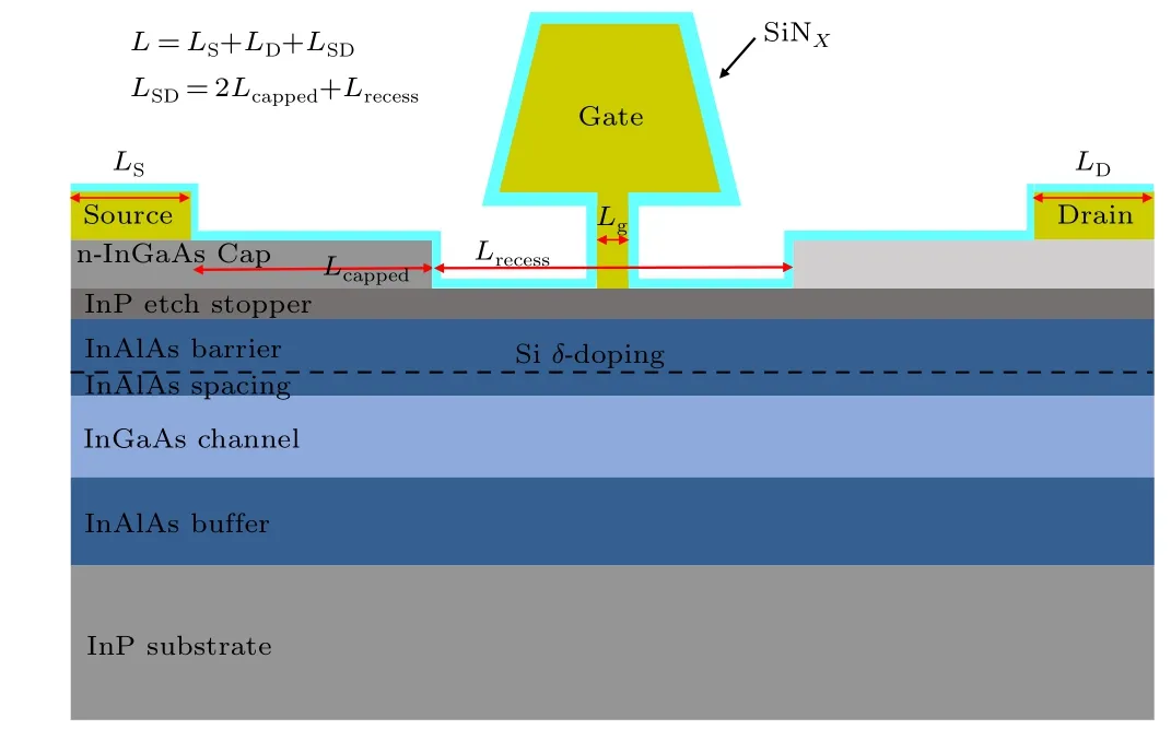
Fig.1. Schematic diagram of cross-section of InP-based HEMTs.
Finally, the SiO2hard mask was removed by HF solution and the devices were passivated by a 20-nm SiNxlayer,and then the Ti/Au(15/300 nm)connection pads were evaporated for on-wafer DC and RF characteristics measurements,as shown in Fig. 2(c). The scanning electron microscope(SEM)images of the present InP HEMT devices with variousLrecessare shown in Fig.3.
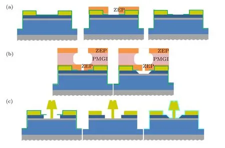
Fig.2. A novel gate-recess technology of InP HEMTs.
The fabrication process of InP HEMTs mainly contains six steps,including mesa isolation,Ohmic contact formation,gate-recess, T-gates, passivation, and connection pads, which is similar to our previous reported devices.[12,13]
Firstly,isolating mesa was formed by means of phosphorus acid-based wet chemical etching. Next, source and drain were spaced 2.4 μm through a lithography process, followed by Ti/Pt/Au (15/15/50 nm) evaporated to satisfy the requirement of Ohmic contact by electron beam evaporation without annealing,with contact resistance measured to be 0.023 Ω·mm and the specific contact resistivity 8.75×10⁻⁸Ω·cm2by TLM method.[14,15]
Afterward,gate-recesses with various width were formed by a novel technology, as shown in Fig. 2. A SiO2layer which was used as hard mask was deposited by PECVD.Then the gate-recesses were defined by electronic beam lithography (EBL) with a ZEP520A e-beam resist layer, and SiO2layer was etched by RIE, as shown in Fig. 2(a). And then the T-gates were defined by EBL with a ZEP/PMGI/ZEP(200/500/200 nm) e-beam resist stack. The top ZEP was exposed by a small dose and wide line and developed by a methyl isobutyl ketone(MIBK):2-butanone(MEK)solution to determine the gate cap, the PMGI was etched by TMAH, and the bottom ZEP was exposed by a big dose and narrow line,then developed by N,N-dimethylacetamide to define the gate foot.And then the cap layers were etched by a phosphate-based solution to form the gate-recesses.As the adhesiveness of the In-GaAs surface to ZEP is rather weaker than that to SiO2,the cap layer beyond the SiO2hard mask could be etched absolutely,as a result,the width of the gate-recess could be controlled by the opening size of the SiO2layer. After the formation of the gate-recess,a Ti/Pt/Au(3/25/300 nm)metal stack was evaporated and lifted off,as shown in Fig.2(b).
Fig. 3. SEM images of the present InP HEMT devices with various Lrecess.(a) InP HEMT device, [(b) and (e)] Lrecess =0.4 μm, [(c) and (f)] Lrecess =0.6μm,[(d)and(g)]Lrecess=0.8μm.
3. Results and discussion
To study the impact of symmetric gate-recess length(Lrecess), the DC and RF characteristics of InGaAs/InAlAs HEMTs were characterized by HP4142 semiconducter parameter analyzer and Agilent E8363B PNA vector network analyzer from 0.1 GHz to 40 GHz at room temperature. After the measurement,theS-parameters were extracted and studied.
3.1. DC characteristics
Figure 4 shows three sets of current-voltage (ID-VDS)curves of InGaAs/InAlAs HEMTs. The devices have variousLrecessof 0.4 μm, 0.6 μm, 0.8 μm and a T-shapedWgof 2×50μm. The devices exhibited excellent pinch-off and current saturation characteristics up toVDS=1.5 V.Kink effect is
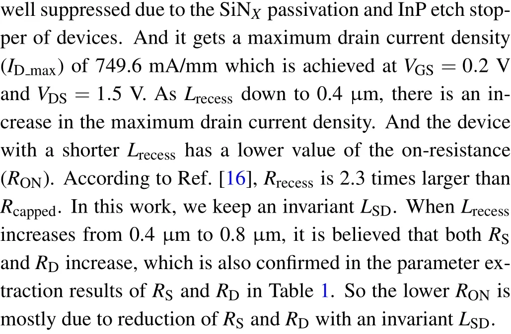

Fig. 4. Output characteristics of InP HEMTs with various Lrecess (Lrecess =0.4,0.6,and 0.8μm).
Figure 5 plots the extrinsic transconductance (gm) characteristics atVDS=1.5 V.The devices exhibit a continuously increasinggmwithLrecessdown to 0.4 μm. According to Eq.(1),it can be explained by the decrease ofRS. The maximum transconductance(gm,max)increases from 941.4 mS/mm atVGS=-0.25 V to 1111 mS/mm atVGS=-0.35 V.
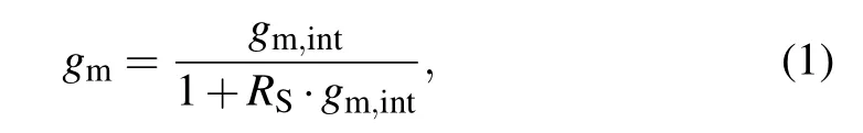
wheregm,intis the value ofgmfor the core part of HEMTs without any parasitic resistances and capacitances. AndRSis the parasitic resistances of source respectively.
Figure 6 plots the transfer characteristics. The drainsource voltage(VDS)is increased from 1.0 V to 1.5 V with step of+0.1 V.A positive threshold voltage(Vth)shift is observed asLrecessincreases. It can be explained the electron density in the channel of the side-etched region is reduced by surface depletion caused by surface states.[17]Generally, the electron density in side-etched region becomes smaller as the threshold voltage(Vth)of the HEMT’s increases.
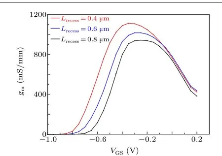
Fig. 5. The extrinsic transconductance (gm) characteristics for InP HEMTs with various Lrecess at VDS=1.5 V(Lrecess=0.4,0.6,and 0.8μm).
Fig. 6. The transfer characteristics for InP HEMTs with various Lrecess(Lrecess=0.4,0.6,and 0.8μm).
3.2. RF characteristics
The devices were measured using on-wafer open and short patterns to subtract pad capacitances and inductances from the measured deviceSparameters,as shown in Ref.[18].Figure 7 shows a measured current gain (H21), maximum available gain, and maximum stable gain (MAG/MSG), and Mason’s unilateral gain (U) against frequency for all devices withLrecess=0.4,0.6,and 0.8μm. The bias condition was atVDS=1.5 V,VGS=-0.2 V.The cutoff frequency(fT)and the maximum oscillation frequency (fmax) were obtained by extrapolating the curve ofH21followed by a slope of-20 dB/dec andUfollowed by a slope of-20 dB/dec. The extrapolatedfTandfmaxare 188 GHz and 1112 GHz atLrecess=0.8 μm,207 GHz, and 723 GHz atLrecess=0.6 μm, 230 GHz, and 555 GHz atLrecess=0.4μm.
ThefTandfmaxare expressed as follows:whereCgsis the parasitic capacitance from gate to source,Cgdis the parasitic capacitance from gate to drain,andRg,RD,andRSare the parasitic resistances of gate, drain, and source respectively. Thegmis the extrinsic transconductance and thegdis conductance between the drain and the source.
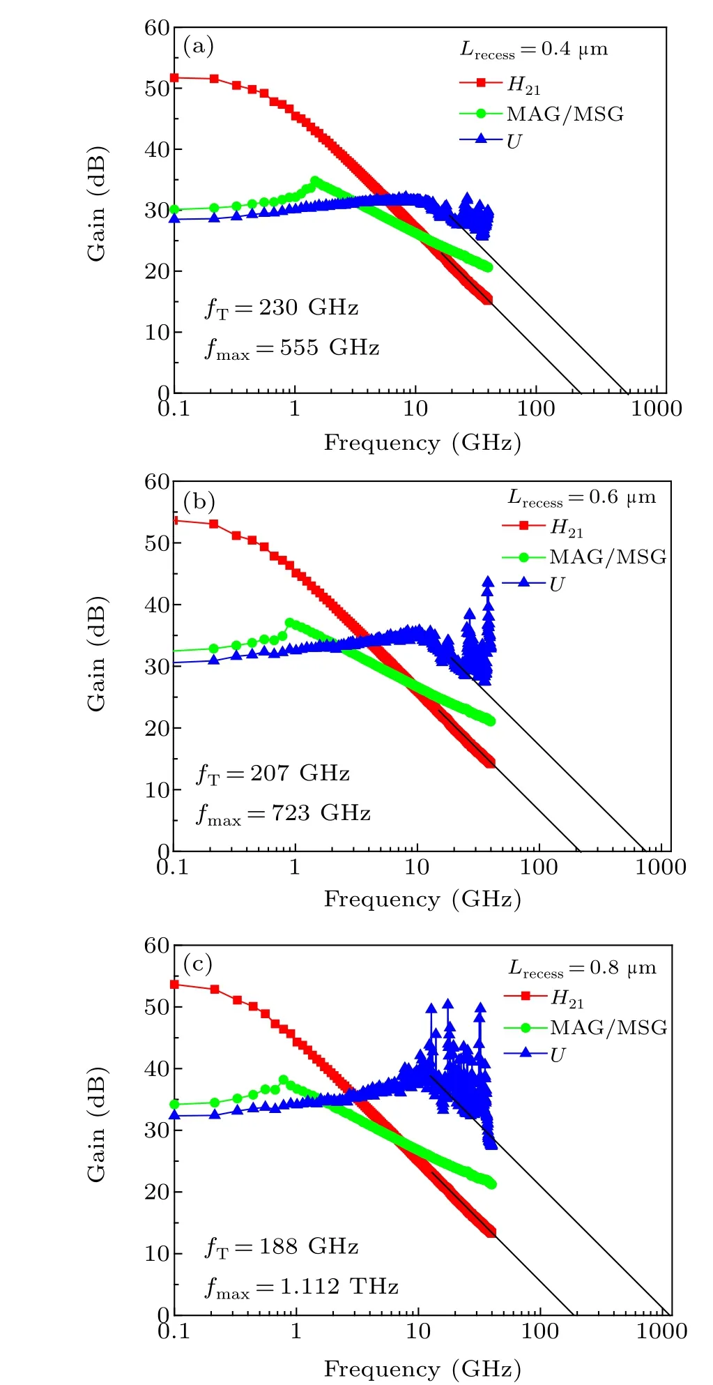
Fig. 7. The measured H21, MAG/MSG, and U gain versus frequency of the HEMT with various values of Lrecess (0.4 μm, 0.6 μm, 0.8 μm) at VGS=-0.2 V and VDS=1.5 V.
As shown in Fig. 8(a),fTdecreases with the increase ofLrecess. Equation (2) shows thatfThas a positive correlation withgm. And thefTwould be good because of the highgm. According to the results ofCgdparameter extraction in Table 1 and Fig. 8(b), asLrecessincreases,Cgdgradually decreases.This is becauseLrecessincreases,leading to a decrease inLcapped. Therefore, the spacing between the cap layer and the gate increases,Cgdgradually decreases. At the same time,Table 1 also shows thatRSandRDincrease with the increase ofLrecess. So we believe that in this work,changing the value ofLrecessmakes the change ofRSandRDhaving a greater impact onfTthan the change of parasitic capacitanceCgd.
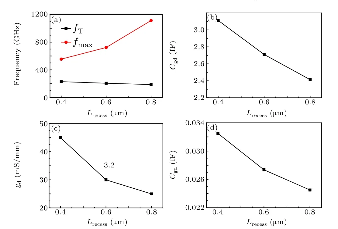
Fig.8. Dependence of fT,Cgd,gd,and Cgd/Cgs on Lrecess for InP HEMTs.
Although the smallerLrecessincreasesfT, figures 8(b)-8(d)show thatCgd,gd,andCgs/Cgddecrease with the increase ofLrecess, which is why the largerLrecessobtains the highestfmax. Since a largeLrecessleads to a decrease ingdandCgs/Cgd, increasingLrecesscan achieve an increase infmax.This is because the increase inLrecessmakes the gate-drain electric field weaker,thereby suppressing impact ionization.[9]Table 1 summarizes the small-signal modeling parameters for the devices with differentLrecess,such asCgs,Cgd,gm,andgd,based on our previous research.[19-21]

Table 1. The parameters of small signal equivalent circuit of devices.
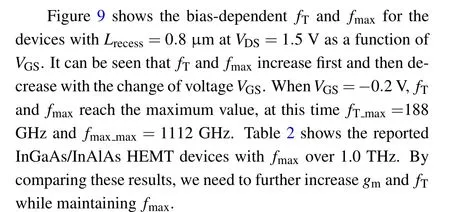
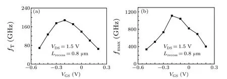
Fig.9. The fT and fmax for InP HEMTs with various VGS at VDS=1.5 V.
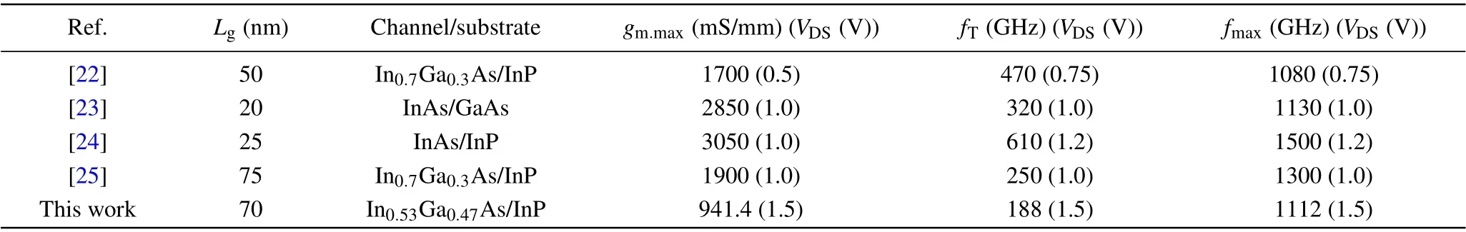
Table 2. Comparison with published InGaAs(InAs)/InAlAs HEMTs with fmax>1.0 THz.
4. Conclusion
In summary, a set of symmetric gate-recess InP HEMT devices with variousLrecesswere fabricated by a novel gaterecess technology. With the increase ofLrecess,fTdecreases andfmaxincreases. WhenLrecessis 0.4μm,the device has the maximumfT=230 GHz,as well as the maximum drain current density and transconductance. WhenLrecessis 0.8μm,the device has a maximumfmax=1112 GHz.
Acknowledgments
Project supported by the National Natural Science Foundation of China (Grant No. 61434006). The authors would like to thank Yan-kui Li for his assistance during the measurements. We are also grateful to all the members of High-Frequency High-Voltage Device and Integrated Circuits Center for their valuable help during the experiment.
猜你喜歡
Chinese Physics B(2023年9期)2023-10-11 07:56:02
Chinese Physics B(2022年10期)2022-10-26 09:54:30
科海故事博覽·上旬刊(2022年5期)2022-05-17 16:17:01
Chinese Physics B(2022年5期)2022-05-16 07:12:16
科技進(jìn)步與對策(2022年2期)2022-02-11 01:59:28
科技進(jìn)步與對策(2020年12期)2020-07-03 07:04:56
華中師范大學(xué)學(xué)報(人文社會科學(xué)版)(2020年3期)2020-06-17 09:02:16
岷峨詩稿(2019年4期)2019-04-20 09:02:10
Acta Mathematica Scientia(English Series)(2018年5期)2018-11-22 09:24:04
童話世界(2017年34期)2017-12-04 09:09:48

- Chinese Physics B的其它文章
- Role of compositional changes on thermal,magnetic,and mechanical properties of Fe–P–C-based amorphous alloys
- Substrate tuned reconstructed polymerization of naphthalocyanine on Ag(110)
- Anti-PT-symmetric Kerr gyroscope
- Information flow between stock markets:A Koopman decomposition approach
- Cascading failures of overload behaviors using a new coupled network model between edges
- High efficiency ETM-free perovskite cell composed of CuSCN and increasing gradient CH3NH3PbI3