
Impact of gate offset in gate recess on DC and RF performance of InAlAs/InGaAs InP-based HEMTs
2022-05-16 07:12:16ShuruiCao曹書睿RuizeFeng封瑞澤BoWang王博TongLiu劉桐
Chinese Physics B 2022年5期
關(guān)鍵詞:王博
Shurui Cao(曹書睿) Ruize Feng(封瑞澤) Bo Wang(王博) Tong Liu(劉桐)
Peng Ding(丁芃)1,2,?, and Zhi Jin(金智)1,2,?
1High-Frequency High-Voltage Device and Integrated Circuits Center,Institute of Microelectronics,Chinese Academy of Sciences,Beijing 100029,China
2University of Chinese Academy of Sciences,Beijing 100029,China
3Guangxi Key Laboratory of Precision Navigation Technology and Application,Guilin University of Electronic Technology,Guilin 541004,China
Keywords: InP HEMT,InGaAs/InAlAs,cut-off frequency(fT),maximum oscillation frequency(fmax),asymmetric gate recess
1. Introduction
Due to high frequency, high gain, low power consumption, and low noise performance, InP-based high electron mobility transistors (HEMTs) are one of the most promising semiconductor devices for millimeter-wave and terahertz monolithic integrated circuits.[1–5]The excellent performance is attributed to high carrier density, high electron velocity, and low gate leakage current. A cutoff frequency (fT)of over 700 GHz using 25-nm gate was reported in InPbased HEMTs[6]. A maximum oscillation frequency (fmax)of 1.5 THz and a terahertz IC operating at 1 THz using 25-nm gate InP-based HEMTs were demonstrated.[7]ThefTandfmaxof HEMTs were mainly improved by scaling down the gate length of devices.[8]On the other hand,it is of great significance to optimize parasitic effects in order to further improve performance.[9]By reducing the source-to-drain space,parasitic resistance was suppressed and RF performance was improved.[10,11]Modifying the gate recess is another effective way to improve high-frequency characteristics of InP-based HEMTs. The adoption of asymmetric gate recess was proved helpful to improvefmax.[12,13]On this basis,we would like to further investigate the impacts of asymmetric gate recess by varying the gate location in the recess.
In this paper,we will report on how the gate offset in gate recess impacts the DC and RF characteristics of InP-based HEMTs instead of a gate scaling down that is often used to obtain high performance. We designed and fabricated a set of devices,of which the gate location was varying in the recess.Therefore,various forms of asymmetric gate recess were realized. A fixed source-to-drain space was maintained at 2.4 μm for the same periphery conditions. The gate was located at the recess center,with an offset toward source or drain side to form the whole gate structure. The gate recess lengthLrecessis expressed asLrs+Lg+Lrd,whereLrsis the source-side recess length,Lgis the gate length, andLrdis the drain-side recess length. It is easy to adjust the gate location through one step EBL after the recess is defined and form the asymmetry of gate recess. To draw a general conclusion,gate recesses were defined with three lengths, which were 0.4 μm, 0.6 μm, and 0.8 μm respectively. It was found that the gate away from drain side was effective in decreasing parasitic source resistance, output conductance and gate-to-drain capacitance, and hence improved transconductance andfmaxeven though an increase ofCgsis not ideal for a highfT.
2. Device fabrication
Figure 1 shows the cross-section schematic diagram of the device with a gate offset toward source side. Epitaxial layer structures of InP-based HEMTs were grown on a 3-inch(1 inch=2.54 cm)semi-insulating InP(100)substrate by gas source molecular beam epitaxy (GSMBE). The layers, from bottom to top, were composed of a 500-nm In0.52Al0.48As buffer layer, a 15-nm lattice matched In0.52Ga0.48As channel layer, a 3-nm In0.52Al0.48As spacer layer, an Si planar doping with a sheet carrier density of 5×1012cm-2,an 8-nm In0.52Al0.48As Schottky barrier layer, a 4-nm InP etch-stop layer, and a 15-nm/15-nm/10-nm heavily Si-doped In0.52Ga0.48As/In0.53Ga0.48As/In0.65Ga0.35As composite cap layer with a concentration of 1×1019cm-3/1×1019cm-3/3×1019cm-3. Hall measurement was carried out at room temperature. The two-dimensional electron gas (2DEG) carrier mobility was 12000 cm2/(V·s).
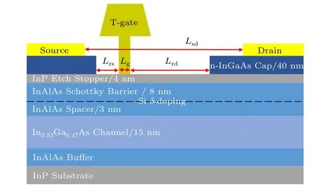
Fig.1. Cross-section schematic diagram of the InP-based HEMT with a gate offset toward source.
The fabrication process of InP-based HEMTs consisted of four main steps,namely mesa isolation,Ohmic contact formation, gate recess, and T-shaped gate process, which was similar to our previously reported devices.[14]At first isolated mesa was formed to define the area of a device by means of phosphorus acid based wet chemical etching down to buffer layer. Then source and drain were defined by lithography with a 2.4-μm space in between. Ohmic contacts were formed using electron beam evaporated Ti/Pt/Au(15 nm/15 nm/50 nm)without annealing. The ohmic contact resistivity was measured to be 0.023 Ω·mm and the specific contact resistivity to be 8.75×10⁻⁸Ω·cm2by transmission line method(TLM).[15]Afterward, SiO2was deposited by PECVD, which served as a hard mask for gate recess and improved adherence of photoresist. A novel gate recess process was proposed,where the gate recess was defined by electron beam lithography with a ZEP520A e-beam resist independently of the gate electrode. SiO2mask was etched by reactive ion etching (RIE).For extending investigation, the gate recesses were designed with three different lengths, which were 0.4 μm, 0.6 μm,and 0.8 μm respectively. The gate recess, as a whole, was closer to the source side in order to achieve a higher breakdown voltage. This was followed by T-shaped gate lithography. The gate was defined by EBL with a ZEP/PMGI/ZEP(200 nm/500 nm/200 nm)tri-layer e-beam resist.Here the gate could be located at the recess center,or with an offset toward source/drain, which corresponded to the variation ofLrsandLrd. After pattern definition,wet chemical etching was used to form the gate recess and Ti/Pt/Au(3 nm/15 nm/300 nm)stack layers were evaporated and lifted off to form the T-shaped gate in sequence. Finally the SiO2hard mask was removed,the devices were passivated by a 20-nm SiNxlayer,and Ti/Au(15 nm/30 nm)connection pads were evaporated for on-wafer characterization.The SEM images of the devices are shown in Fig.2.
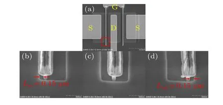
Fig.2. SEM images of InP HEMTs with gate offsets in gate recess: (a)top view of InP HEMT; (b) gate offset toward source; (c) gate in the middle of recess;(d)gate offset toward drain.
3. Result and discussion
In a narrow recess the absolute value of gate offset was relatively small while in a wider recess the offset was larger.The offsets from recess center were±0.05 μm,±0.15 μm,and±0.25 μm for recess lengths of 0.4 μm,0.6 μm,and 0.8 μm,respectively. In this case,Lrswas kept at 0.15 μm for gate offset toward source andLrdwas kept at 0.15 μm for gate offset toward drain. The values of gate offsets were normalized as-1, 0, and 1 to represent the offset toward source, in the middle,and toward drain,respectively.
3.1. DC characteristics
On-wafer DC measurement was carried out by a HP4155A semiconductor parameter analyzer at room temperature. The gate–source voltage(Vgs)was swept from-1.0 V to 0.2 V at a step of +0.1 V, and the drain–source voltage (Vds) was from 0 V to 1.5 V. The threshold voltage was about-0.6 V. These devices exhibited a maximum saturated drain currentIds,maxof 763.9 mA/mm atVGS= 0.2 V andVgs=1.5 V,which was achieved in a device of 0.4-μm recess length.The maximum extrinsic transconductance,gm,max,was high up to 1120 mS/mm atVGS=-0.25 V.
Devices with a wider gate recess,where the absolute gate offset was larger,indicated clear changes ofIdsandgm. WhenLrsdecreased, namely gate location shifted from drain side to source side, bothIds,maxandgm,maxincreased. Figure 3 plots theIds–Vdscurves of 0.8-μm-recess devices with different gate offsets, and theIds,maxincreased by over 15% from 541 mA/mm to 621 mA/mm. Another benefit could be found that a longerLrdlead to effective suppression of impact ionization when a largeVdswas applied. ForVgs=-0.4 V, the drain current of positive-offset device exceeded that of zerooffset device atVdsover 1.2 V, illustrating a weaker impact ionization in longer distance between gate and drain. Besides,gm,maxincreased by 17%from 864 mA/mm to 1016 mA/mm,as is shown in Fig. 4. Extrinsic transconductancegmcan be expressed as
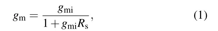
wheregmiis the intrinsic transconductance removing the influence of parasitic parameters, andRsis the parasitic source resistance. Since recess resistanceRrecessis 2.3 times larger than that of cap layerRcap,[12]a smallerLrsin the access region between gate and source led to a smallerRsthat improved extrinsic transconductance. The voltage drop onRswas reduced, and consequently more proportion ofVgsdropped on the Schottky barrier capacitor for gate control.connection pads.fTwas obtained by extrapolating H21curve to unit gain by a slope of-20 dB/decade. Moreover, due to the noisy characteristics of unilateral gain(U)which indicated insufficient estimation offmaxvariation,MAG/MSG was used to extrapolatefmax,[13–16]as is shown in Fig.5. SincefTandfmaxhad a positive correlation withgmi,VdsandVgswere biased at 1.5 V and-0.2 V,respectively,which were associated with the maximumgmiin our devices.As can be seen in Fig.6,fmaxranged from 374 GHz to 584 GHz whilefTranged from 167 GHz to 225 GHz, and there was a trade-off between the two parameters.The highestfTwas obtained from the positive gate-offset device with 0.4-μm gate recess while the highestfmaxwas obtained from the negative gate-offset device with 0.8-μm gate recess.
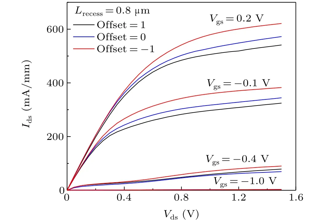
Fig.3. Output characteristics of 0.8-μm-recess HEMTs.
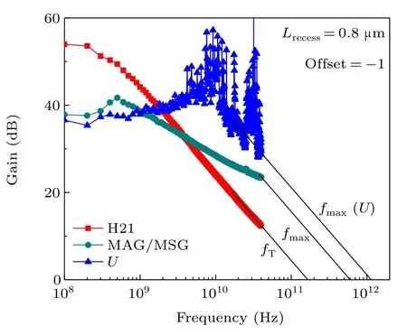
Fig.5. Extrapolation of fT and fmax from measured data.
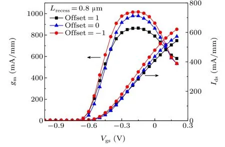
Fig.4. Transfer characteristics of 0.8-μm-recess HEMTs.
Moreover,for all devices of different gate recess lengths,gmshowed a maximum value when gate was located with an offset toward source. And the correspondingIdstend to be a larger value due to better gate control.
3.2. RF characteristics
RF characteristics were measured on wafer by Agilent E8363B PNA vector network analyzer from 0.1 GHz to 40 GHz at a step of 0.1 GHz. Open-short patterns were fabricated on the same wafer forSparameter deembedding of
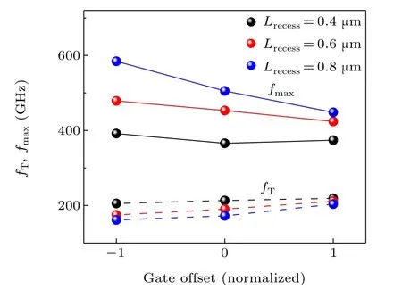
Fig.6. fT and fmax of HEMTs with gate offsets in gate recess(solid: fmax,dashed: fT).
The results were similar for devices with three different gate recess lengths. When the normalized gate offset varied from 1 to-1, which literally meant that the gate location moved from drain side to source side,fTdecreased,andfmaxincreased. It can be seen from Fig.6 that in wide recesses,the ratio offTandfmaxchange became more obvious.fTandfmaxcan be expressed as
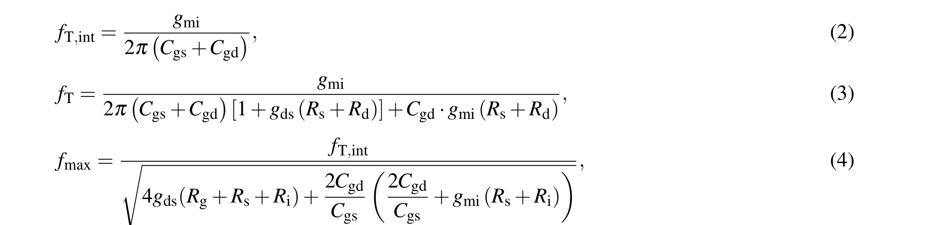
wheregmiis the intrinsic transconductance,Cgsis the gate–source capacitance,Cgdis the gate–drain capacitance,gdsis the output conductance,Rsis the source resistance,Rdis the drain resistance,Rgis the gate resistance, andRiis the intrinsic resistance in the channel region.[16]fT,intrepresents the cut-off frequency of the intrinsic part of HEMTs without parasitic resistance and capacitance. Parameters of the small-signal equivalent circuit model were extracted and compared based on Rorsman’s method[17]and our previous research.[18–20]Figure 7 illustrates the changes in key parameters, and Table 1 lists some related small-signal model parameters of 0.8-μm-recess devices. The small-signal model was then simulated with extracted parameter values. Figure 8 shows a good fitting result of our small-signal model compared with the measured data after de-embedding,which indicated effectiveness and accuracy of our extracted parameters.
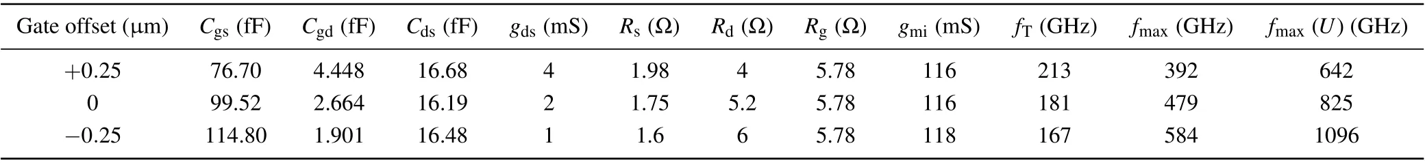
Table 1. Parameters of small-signal model for InP HEMTs of 0.8-μm gate recess.
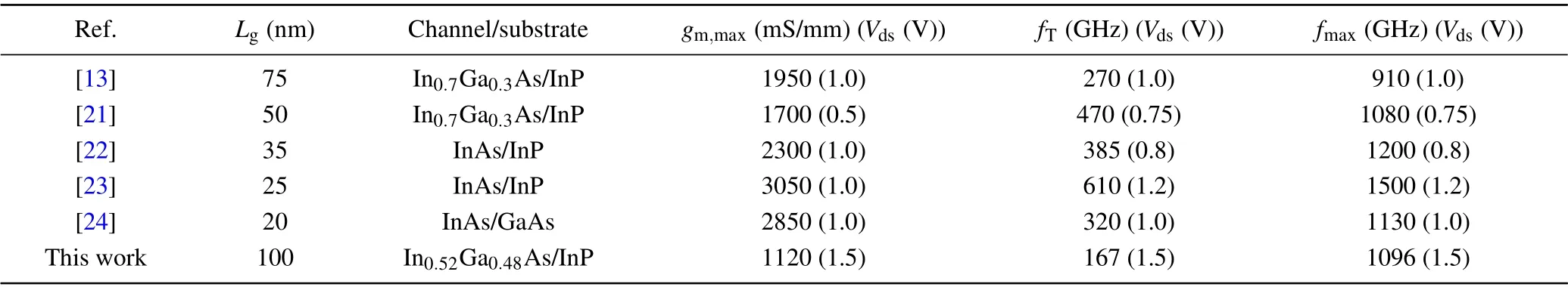
Table 2. Benchmarks of fmax in InGaAs/InAlAs HEMTs.
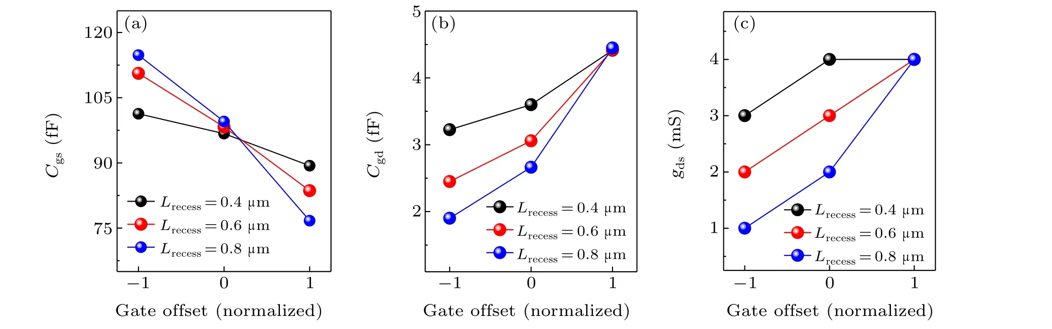
Fig.7. Extracted small-signal parameters of HEMTs with different gate offsets: (a)gate–source capacitance;(b)gate–drain capacitance;(c)output conductance.
For a given gate recess,whereLrs+Lrdwas a constant,the variation of gate offset from drain side to source side meant a smallerLrsand a largerLrd.CgsandCgdwhich were related to the corresponding space consequently changed,resulting inCgsincrease andCgddecrease. Thegdsdecrease was also attributed to the extension ofLrd.[13]Here the electric field between gate and drain was smoothed, and thus impact ionization in the channel was suppressed. This was consistent with the phenomenon observed in DC measurement.
AlthoughCgsandCgdchanged in a contrary way,the absolute value ofCgswas still much larger than that ofCgd. As a result,Cgs+Cgdin total increased, contributing to the decrease offT. As forfmax, although it was proportional tofT,Cgd/Cgsfurther decreased due to the contrary change,leading to the reduction in the denominator of thefmaxformula by a greater ratio. Moreover, according to Eq. (4), the reduction ofgdsandRswas helpful in increasingfmaxas well. As is plotted in Fig. 5, a highfmaxof approximately 1.1 THz was achieved from extrapolation of Mason’s unilateral gain,U,to 0 dB when aVgsof-0.2 V and aVdsof 1.5 V were applied to the HEMT.
Table 2 shows the benchmarks offmaxin published papers.[13,21–24]In some cases,fmaxexceeding 1 THz was obtained by scalingLgto less than 50 nm. Meanwhile,the InPbased HEMT reported in this paper reached afmaxof approximately 1.1 THz althoughLgwas relatively large at 100 nm.
In a multi-function MMIC, devices of various performance are needed. For instance, an analog module requires highfTwhile a power amplifier requires highfmax. Thus,the device requirements can be satisfied by simply adjusting the gate location in gate recess. Furthermore,by adding the modification of gate recess length,various transistor performances are available over a larger range.
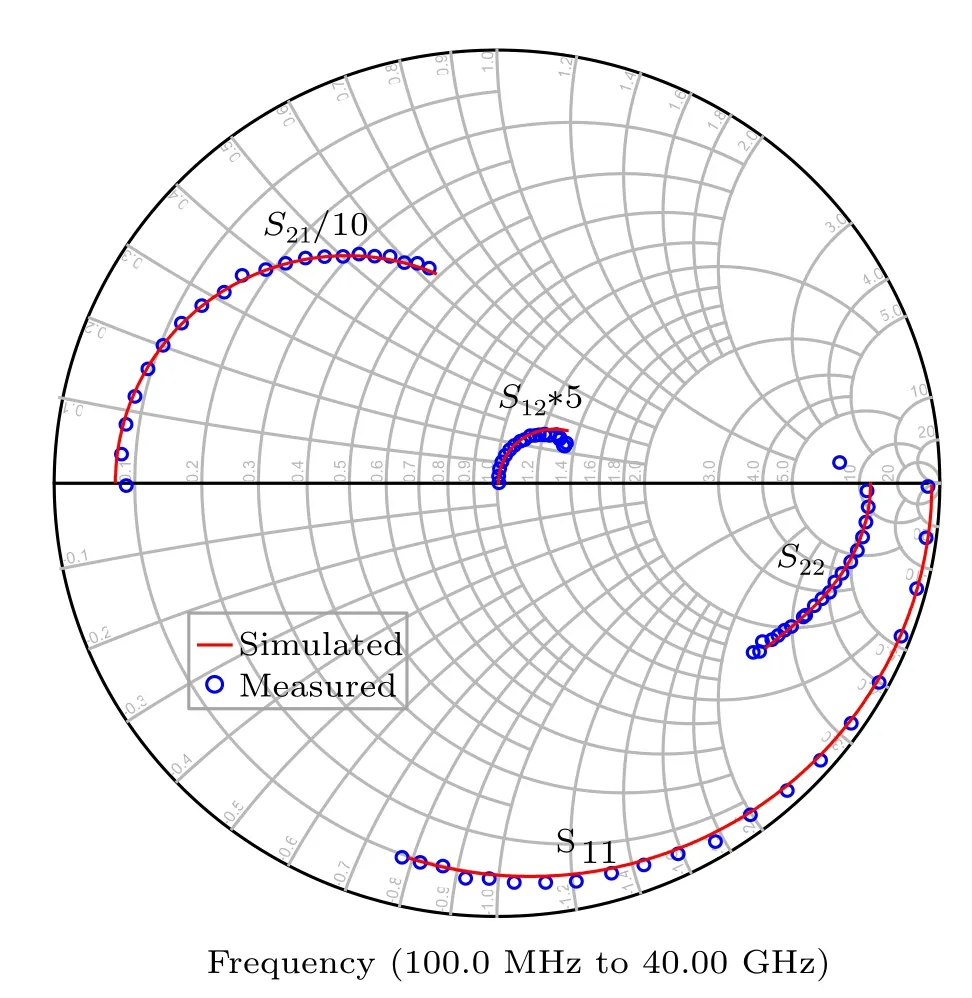
Fig. 8. Small-signal model versus de-embedded S parameters of InP-based HEMTs (red line: small-signal model; blue dot: de-embedded measured S parameters).
4. Conclusion
In this paper, we investigated a set of 100-nm InP-based HEMTs with gate offsets in the gate recess. A novel technology was proposed for independent definition of gate recess and T-shaped gate. As a result,a maximumIdsof 769 mA/mm andgmof 1120 mS/mm were obtained. When the gate offset varied from toward drain side to toward source side,Idsandgmincreased. The reduction ofRsimproved extrinsic transconductance and decreased the voltage drop split fromVgs. In the meantime,fTdecreased whilefmaxincreased. Afmaxof 1096 GHz was obtained in a 0.8-μm-recess HEMT with a gate offset toward source side. This was attributed to the increase ofCgs, along with the reduction ofCgd,gds, andRs. This work provides simple and flexible device parameter selection for HEMTs of different usage over a large frequency range.
Acknowledgment
Project supported by the National Nature Science Foundation of China(Grant No.61434006).
猜你喜歡
Chinese Physics B(2023年9期)2023-10-11 07:56:02
Chinese Physics B(2022年10期)2022-10-26 09:54:30
科海故事博覽·上旬刊(2022年5期)2022-05-17 16:17:01
Chinese Physics B(2022年5期)2022-05-16 07:12:20
科學(xué)家(2022年4期)2022-05-10 03:47:14
Chinese Physics B(2022年1期)2022-01-23 06:35:18
Plasma Science and Technology(2021年11期)2021-11-30 08:28:50
知音海外版(上半月)(2019年7期)2019-01-10 06:57:30
Acta Mathematica Scientia(English Series)(2018年5期)2018-11-22 09:24:04
速讀·下旬(2017年4期)2017-06-20 17:51:03

- Chinese Physics B的其它文章
- Erratum to“Boundary layer flow and heat transfer of a Casson fluid past a symmetric porous wedge with surface heat flux”
- Erratum to“Accurate GW0 band gaps and their phonon-induced renormalization in solids”
- A novel method for identifying influential nodes in complex networks based on gravity model
- Voter model on adaptive networks
- A novel car-following model by sharing cooperative information transmission delayed effect under V2X environment and its additional energy consumption
- GeSn(0.524 eV)single-junction thermophotovoltaic cells based on the device transport model