
Temperature-dependent subband mobility characteristics in n-doped silicon junctionless nanowire transistor?
2019-06-18 05:42:38YaMeiDou竇亞梅WeiHuaHan韓偉華YangYanGuo郭仰巖XiaoSongZhao趙曉松XiaoDiZhang張曉迪XinYuWu吳歆宇andFuHuaYang楊富華
Chinese Physics B 2019年6期
關(guān)鍵詞:富華
Ya-Mei Dou(竇亞梅),Wei-Hua Han(韓偉華),?,Yang-Yan Guo(郭仰巖),Xiao-Song Zhao(趙曉松),Xiao-Di Zhang(張曉迪),Xin-Yu Wu(吳歆宇),and Fu-Hua Yang(楊富華),3
1Engineering Research Center for Semiconductor Integration Technology&Beijing Engineering Center of Semiconductor Micro-Nano Integrated Technology,Institute of Semiconductors,Chinese Academy of Sciences,Beijing 100083,China
2Center of Materials Science and Optoelectronics Engineering,University of Chinese Academy of Sciences,Beijing 100049,China
3State Key Laboratory for Superlattices and Microstructures,Institute of Semiconductors,Chinese Academy of Sciences,Beijing 100083,China
Keywords:effective subband mobility,thermal activation,Coulomb scattering,silicon nanowire transistor
1.Introduction
The metal-oxide-semiconductor field-effect transistor(MOSFET)has kept pace with Moore’s law by improving the “performance/power”ratio since 2000.New materials,such as strained silicon,[1]high-k dielectric and metal gate electrodes,[2]are introduced in the complementary metaloxide-semiconductor(CMOS)process to increase the carrier mobility.However,as the space of pn junctions in source and drain drops to less than 10 nm,there is a great challenge in the fabrication of pn junctions with heavily doping concentration gradients.In recent years,the silicon junctionless nanowire transistor(JNT)with uniform doping in source,drain,and channel has attracted much attention due to the simple fabrication and unique properties,in which the narrow conduction channel emerges in the axis of the silicon nanowire.Compared with the inversion-mode transistors,JNTs have less degradation of mobility and more apparent quantum-confinement effects on carrier transport.[3,4]Therefore,it is necessary to understand the strong oscillatory behaviors of carrier effective mobility in the quantized subband structure.Yamada et al.estimated the subband mobility of quasi-two-dimensional electrons in Si atomic layer doped GaAs for the first time,in which the subband mobility difference was up to 20:1.[5]Each new subband filling results in an increased intersubband Coulomb scattering,thus a reduced mobility.Colinge et al.measured the subband mobility of trigate silicon-on-insulator(SOI)MOSFETs to reach about 1200 cm2/(V·s)due to screening of impurity scattering at the temperature of 4.4 K,which decreases as temperature increases.[6]The Coulomb scattering is temperature-dependent for thermally activated carriers between impurity band and conductive subbands.Yi et al.observed quantum confinement effects of sub-5-nm thick p-Si junctionless nanowire(NW) field-effect transistors(FETs)at room temperature.[4]The hole mobility is increased in p-SiNW FETs,which is caused by minimal acoustic phonon assisted intersubband scattering.In this paper,we investigate temperature-dependent effective mobility characteristics in impurity band and conduction subbands of n-doped silicon JNT.Interestingly,the electron effective mobility of conduction subbands has a maximum value at low temperatures,which relates to the minimum electron effective mobility of the impurity band.The effective subb and mobility is temperaturedependent on the electron interactions by thermal activation,impurity scattering,and intersubband scattering.
2.Device fabrication and characterization
The device in Fig.1(a)was fabricated on the(100)-orientated SOI wafer,with the top silicon thickness of 55 nm and buried oxide layer of 145 nm.First,the top silicon layer was implanted under SiO2buffer layer with 33-keV arsenic ions at a dose of 2×1012cm-2.Following the implantations,the silicon nanowire along the 〈110〉direction was defi ned by electron beam lithography(EBL)and reactive ion etching(RIE).The width of the nanowire was about 60 nm,which was measured by scanning electron microscope(SEM).Then the silicon nanowire was oxidized at 900°C for 10 min in dry oxygen ambience to form an SiO2layer.Next,SiO2layer was removed by buffered oxide etcher(BOE)for 40 s to reduce the size of silicon nanowire and remove the etching damage.Subsequently,the 22-nm-thick gate dielectric layer was generated on the surface of silicon nanowires by thermal oxidation.The 200-nm-thick undoped polysilicon layer was then deposited by low-pressure chemical vapor deposition(LPCVD).The polysilicon layer was oxidized at 900°C for 30 min in oxygen ambience to form a 15 nm-thick SiO2layer.The poly-Si layer was implanted with 33-keV boron ions at the dose of 2×1012cm-2,followed by furnace annealing at 1000°C for 15 s.Following the implantations,the polycrystalline gate pattern was de fined by EBL and inductively couple plasma(ICP)etching.Then,a 200 nm-thick SiO2passivation layer was deposited by LPCVD.Finally,the source,drain,and gate electrodes were fabricated.Figure 1(b)shows the top view SEM image of the device.We measured the JNT electrical characterization with an Agilent B1500 A semiconductor parameter analyzer within the temperature range from 6 K to 250 K.
3.Results and discussion
Figure 2 shows the measured drain current Idsin the JNT device as a function of gate voltage Vgand temperatures at the bias Vds=10 mV in both linear and log scales.Clear oscillatory peaks and several step-like drain current features are observed at the initial stage of the Ids-Vgtransfer characteristics,implying the evolution of electron transport behaviors from quantum dots to quantum wire.The initial drain current below the gate voltage of about 2.3 V flows through an ultranarrow channel in the center axis of silicon nanowire,in which several ionized dopant atoms work as quantum dots in an array.With the gate voltage increasing,the dopant barrier potentials are reduced in the wider channel,thereby enhancing the coupling of dopant-induced quantum dots.The Fermi energy level is allowed to enter the conduction subbands in the quantum con fined one-dimensional channel.The step-like current features at the gate voltages of around 2.5 V and 2.8 V result from the successive filling of individual subband.Each current step corresponds to the filling of a new subb and.However,as the temperature increases up to 100 K,the current oscillation features gradually decrease and disappear due to the weak potential confinement in conduction channel.
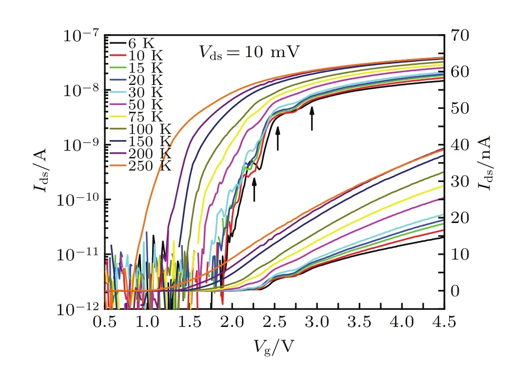
Fig.2.Drain current Idsversus gate voltage Vgwith bias Vds=10 mV at different temperatures.
Figure 3(a)shows that several remarkable oscillation peaks at initial conductance varies with the gate voltage within the temperature range from 6 K to 50 K,which are successively shifted in the conductance for clarity.Only one oscillation peak is observed at the temperature of 6 K,which results from electron tunneling through the level in only one donor-induced quantum dot.Under the gate electric field,the electrons self-consistently fill in the D-level state of the neutral donor atom,which is much closer to the top of the barrier along the transport direction due to screened donor potential.[7]As the temperature rises,thermally activated electrons are able to hop through the optimal neighbor dopant atoms.Several split peaks are observed in the temperature range from 10 K to 50 K in Fig.3(a),resulting from the coupling effect in the dopant-induced quantum dot array.To show this more clearly,the drain current Idsand transconductance gmcurves are presented in Fig.3(b)as a function of gate voltage Vgin different biasVdsfrom 3 mV to 10 mV at the temperature of 30 K.Two groups of double oscillation current peaks can be observed at the gate voltage of 1.95 V and 2.13 V,resulting from the electrons tunneling through the D0and D-states of the two ionized donors.As a result,according to the spacing of the gate voltage ΔVgs=0.18 V between the D0and D-states of current peaks,we estimate the gate capacitance Cg=e/ΔVgs=0.89 aF for single dopant-induced quantum dot with the potential radius of 1.54 nm.
Figure 4 provides three remarkable temperaturede pendent peaks of the transconductance gm(=?Ids/?Vg|Vds=const),which are extracted from the temperaturede pendent transfer characteristic curves in Fig.2.It can be observed that the gm-peak positions in the gate voltage Vgare basically stable with the temperature increasing,corresponding to the step positions of the drain-current Ids.At the temperature of 6 K,the first transconductance peak at the gate voltage of about 2.13 V originates from the electron tunneling through the D-level of dopant-induced quantum dots.The second and third transconductance peaks at the gate voltages of about 2.44 V and 2.86 V correspond to the electron one-dimensional transport in the first and second conduction subbands,which are the lowest subbands respectively in the 2-fold perpendicular valleys and the 4-fold in-plane valleys of the strain silicon nanowire.[8]

Fig.3.(a)The conductance G varies with the gate voltage Vgin Vds=10 mV at different temperatures.The curves are successively shifted in the conductance for clarity.(b)The transconductance gmversus the gate voltage Vgand the transfer characteristic curve Ids-Vgin Vds=3 mV-10 mV at the temperature of 30 K.

Fig.4.Temperature-dependent transconductance gm-Vgcurves,which are successively shifted for clarity.
In order to understand the interaction mechanism between the impurity band and the conduction subbands,we further investigate the dependence of effective electron mobility on the temperatures.Similar to the definition of the effective electron mobility in inversion-mode MOSFETs in the triode operation regime,the effective mobility in linear accumulation regime of the silicon JNT can be estimated by[4,9-11]
where Lg=280 nm is the gate length,Cox=1.56×10⁻⁷F/cm2is the gate capacitance per unit area,and the effective widthWeffis de fined as twice the height H,plus the width W of nanowire.Figure 5 shows the evolution of the effective mobilities as a function of temperature for the impurity band and conduction subbands(in the inset).It can be observed that the effective electron mobilityμe0at the D-level in the impurity band is the lowest at the temperature of 10 K,in which the thermally activated electrons are delocalized from the ionized donor atoms.The effective electron mobilityμe0of the impurity band is reduced below 10 K by the impurity Coulomb scattering,and then enhanced above 10 K by the increased thermal activation energy of electrons.Therefore,the lowest effective mobilityμe0at 10 K results from the interaction of thermal activation and impurity scattering.[10]As a result,the concentration of activated electrons hopping into the conduction subbands rapidly increases with the temperature increasing.
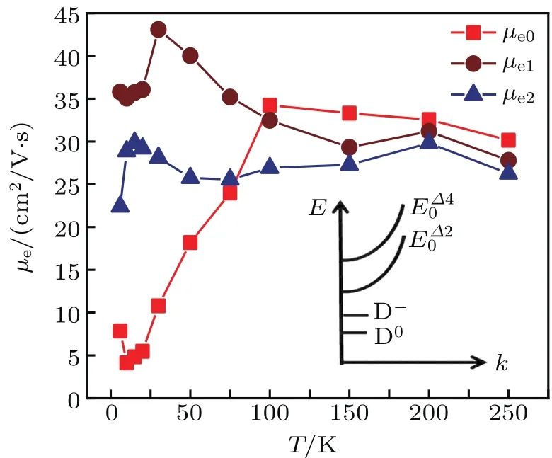
Fig.5.The temperature-dependent effective mobilities of the impurity band and the conduction subbands.The inset is the diagram of the energy band.
The effective subb and mobilitiesμe1and μe2have the largest value at the temperature of 30 K and 15 K,respectively,due to the increased electron concentration and intersubband Coulomb scattering.The effective subband mobility enhancement is attributed to the increase of activated electrons in the occupancy of conduction subbands.[12]The effective mobilityμe1in the first subband is higher than the μe2in the second subband,because the effective electron mass in 2-fold valleys is lower than that in 4-fold valleys. The successive filling of individualsubband strengthens the intersubband scattering with Fermi energy moving up,further reducing the effective subband mobilities.It is also interesting that the effective mobility of impurity band is higher than that of subbands as the temperature is higher than 100 K,which is attributed to the phonon scattering.This means that the intersubband Coulomb scattering of conduction subbands is stronger than that of the impurity band when the phonon interaction is dominant.The phonon-limited mobilities show the slowly declined tendency with temperature increasing above 100 K.
4.Conclusions
In conclusion,we have demonstrated the temperature dependence of effective mobility in impurity band and conduction subbands of the n-type junctionless silicon nanowire transistor.The minimum effective mobility of impurity band at the temperature of 10 K results from the interaction of thermal activation for electrons and impurity scattering.The electron effective mobility of the first subband in 2-fold valleys is higher than that of the second subband in 4-fold valleys.The maximum effective subband mobility at the low temperature is attributed to increased electron concentration and intersubband Coulomb scattering.It is found that the phonon scattering plays a dominant role in both impurity band and conduction subbands above the temperature of 100 K,leading to a slow decline in electron effective mobility.
Acknowledgment
The authors thank Mr.Li Xiao-Ming,Dr.Zhang Yan-Bo,Ma Liu-Hong,and Wang Hao for their technical support in device fabrication.
猜你喜歡
瘋狂英語·新讀寫(2022年12期)2022-12-15 13:50:16
Chinese Physics B(2022年1期)2022-01-23 06:35:10
考試與評(píng)價(jià)·七年級(jí)版(2021年5期)2021-08-14 21:22:27
——專訪富華國(guó)內(nèi)銷售部部長(zhǎng)古嘉杰
專用汽車(2020年11期)2020-11-23 09:24:58
——訪富華銷售總監(jiān)張航博士
專用汽車(2020年10期)2020-10-26 01:11:48
Chinese Physics B(2019年10期)2019-11-06 00:46:08
專用汽車(2016年11期)2017-01-11 02:31:40
專用汽車(2016年5期)2016-03-01 04:14:46
專用汽車(2015年4期)2015-07-08 03:21:04
——走進(jìn)廣東富華重工制造有限公司
專用車與零部件(2015年9期)2015-03-16 01:43:23
- Chinese Physics B的其它文章
- Theoretical study of overstretching DNA-RNA hybrid duplex?
- influence of carbon coating on the electrochemical performance of SiO@C/graphite composite anode materials?
- Spin glassy behavior and large exchange bias effect in cubic perovskite Ba0.8Sr0.2FeO3-δ?
- Aging mechanism of GaN-based yellow LEDs with V-pits?
- Magnetotransport properties of graphene layers decorated with colloid quantum dots?
- Nonlocal effect on resonant radiation force exerted on semiconductor coupled quantum well nanostructures?