
Analysis on degradation mechanisms of normally-off p-GaN gate AlGaN/GaN high-electron mobility transistor?
2021-05-06 08:55:22SiDeSong宋思德SuZhenWu吳素貞GuoZhuLiu劉國柱WeiZhao趙偉YinQuanWang王印權(quán)JianWeiWu吳建偉andQiHe賀琪
Chinese Physics B 2021年4期
Si-De Song(宋思德), Su-Zhen Wu(吳素貞), Guo-Zhu Liu(劉國柱), Wei Zhao(趙偉),Yin-Quan Wang(王印權(quán)), Jian-Wei Wu(吳建偉), and Qi He(賀琪)
The 58th Institution of Electronic Science and Technology Group Corporation of China,Wuxi 214000,China
Keywords: high-electron-mobility transistors(HEMTs),stress,degradation,threshold voltage
1. Introduction
AlGaN/GaN high-electron-mobility transistors(HEMTs)have been considered as the next generation power switching devices due to its outstanding combination of high breakdown strength,low ON-state resistance and high on/off ratio.[1–3]A naturally formed two-dimensional electron gas(2DEG)at the interface of AlGaN/GaN by spontaneous and piezoelectric polarization effects leads to a depletion mode device,[4]which is not preferred for circuit design and system reliability. Thus more and more attentions are paid now to the enhancementmode GaN-on-Si power applications.
In recent years,different approaches have been proposed to design enhancement-mode high-electron-mobility transistors (HEMTs), such as a recessed gate structure,[5]or the same structure with metal–oxide–semiconductor (MOS) gate or metal–insulator–semiconductor (MIS) gate[6–8]to achieve low gate leakage current and positive threshold voltage devices, fluorine plasma ion implantation into the AlGaN or GaN to deplete the 2DEG in the channel,[9,10]by introducing a piezo neutralization layer on top of AlGaN barrier layer[11]or by adopting a p-GaN gate to pull up the conduction band of AlGaN at the AlGaN/GaN heterointerface,sometimes also called gate injection transistors.[12]Among these approaches,p-GaN gate solution has been proved to be a promising candidate for its good trade-off between cost and reliability,[13]and the normally-off p-GaN gate AlGaN/GaN HEMTs are already available in the market. However, gate-related reliability research in p-GaN gate HEMTs is limited and the gate breakdown mechanisms have not been reported extensively yet.[14–20]Herein, a completive investigation on the degradation mechanism of the p-GaN gate HEMTs is necessary aiming to push it further into the market of power switching applications.
In this paper,emphasis was put on the I–V characteristics of the device before and after stressing in high voltage drain bias,forward gate bias and reverse gate bias. The degradation mechanism for the forward gate bias stress was analyzed and modeled in detail,illustrating a possible“weak points”in the gate diode structure. The results are meaningful,valuable and provide a guide to realize high voltage and reliable enhanced mode p-GaN Gate AlGaN/GaN HEMT.
2. Device structure and measurement technique
Figure 1(a) depicts the schematic cross section of p-GaN gate HEMTs, The devices are fabricated on 6-inch(1 inch=2.54 cm) p-type Si (111) substrate. The epitaxial structure is grown by means of metal–organic chemical vapor deposition(MOCVD)and features a stack of 3.5-μm-thick GaN buffer on top of the Si substrate, followed by 150-nmthick GaN channel and 15-nm-thick Al15Ga85N barrier.Afterwards,a 70-nm-thick p-GaN was grown by MOCVD with Mg atoms density of 1×1019cm?3,the p-GaN hole concentration is 1×1017cm?3,corresponding to 1%Mg activation rate.The Ti/Au(45 nm/200 nm)gate metal is evaporated on the top of p-GaN to form a Schottky barrier structure, Ohmic contact is formed by deposition of Ti/Al/Ni/Au metal stack with a whole thickness of 270 nm on the source and drain region,150-nmthick SiN is deposited by plasma enhanced chemical vapor deposition(PECVD)as the surface passivation layer. The device under test(DUT)features a gate length Lg=2.5μm,gate-tosource and gate-to-drain spacing Lgs=2.5μm,Lgd=12μm,respectively, and the gate width is 0.18 mm. The microscope photo of fabricated p-GaN gate AlGaN/GaN HEMT is shown in Fig.1(b).
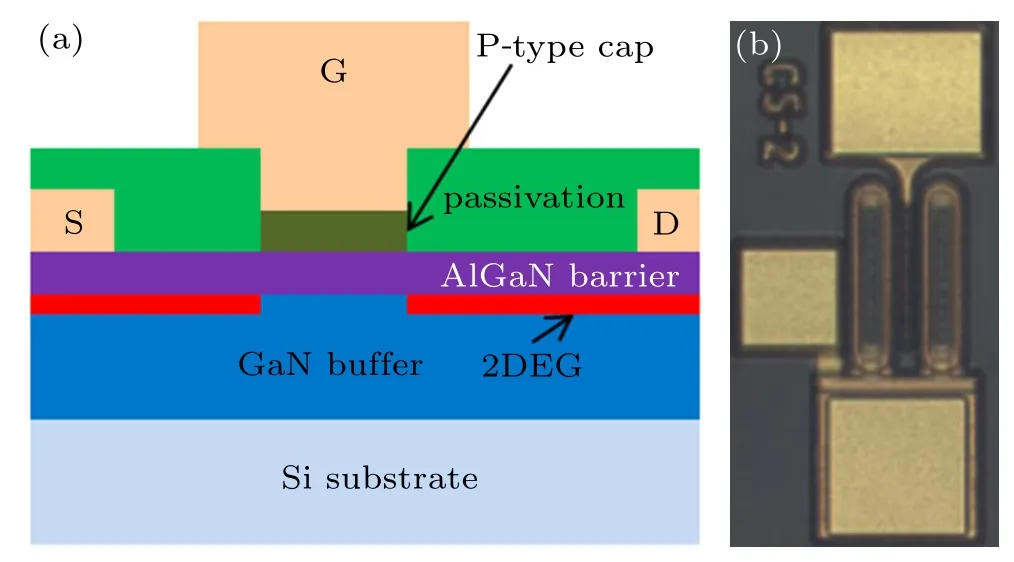
Fig.1.(a)Schematic cross section of the p-GaN gate HEMT;(b)photograph of p-GaN gate HEMT.
On wafer characterization was performed on KEISIGHT B1505,which features in high voltage and high current monitor module,and a probe stage with temperature controller for loading and heating the device. The DUT was summoned to three different stress conditions:high drain voltage bias stress,forward gate bias stress and reverse gate bias stress. Each stress condition is carried out on fresh device,and at least five devices were selected in order to increase the accuracy, for concise of the paper, the electrical characteristics of the most representative devices were monitored and analyzed in details in the following parts.
3. Results and discussion
3.1. High voltage drain stress in off-state
Figure 2(a) depicts the breakdown characteristics of the p-GaN gate AlGaN/GaN HEMT, with drain voltage scanning from 0 V to 800 V, source and gate grounded. The current/voltage of all three terminals (Ig/Vg, the gate current/voltage; ID/Vd, the drain current/voltage; and Is/Vs, the source current/voltage) were monitored, a rapid increase of both Idand Iswere found at drain voltage of about 600 V,indicating the breakdown happens at this point. The threshold voltage is calculated to be 1.5 V by constant current at Id=1μA/mm,as shown in Fig.2(b),while the threshold voltage remains almost unaltered even after a 104-s drain stress at 500 V;The output current atVg=6 V andVd=10 V(Fig.2(c))exhibits a first decrease and then increase behavior with increasing the drain stress voltage. This can be explained by the trapping and de-trapping process, when stressed at moderate voltage,electron is trapped in the SiN/AlGaN interface,as the voltage becomes sufficiently high, a high field-assisted de-trapping process may be initiated.[21]However, this effect is rather small due to the high qualified surface passivation and GaN buffer.
The Ig–Vgcharacteristic is also monitored and described in Fig.2(d),only several nano ampere variations in the reverse gate region was observed,illustrating the P-GaN gate structure was not influenced by the high drain voltage stress.

Fig.2. (a) Breakdown characteristics; (b) transfer characteristic curve; (c) output characteristic curve; (d) gate diode characteristic, before and after drain stress.
3.2. Forward gate bias
In the forward gate bias stress experiment, a large deviation in threshold voltage and output current were observed as shown in Fig.3. The threshold voltage shifts about 0.2 V and 1.5 V toward the negative direction when subjected to forward gate bias stress at Vg=6 V and Vg=7 V for 104s (Tsin the figure denotes stress time),respectively. And the output current calculated at Vg=6 V and Vd=10 V varies 0.7%for Vg=6 V stress and 25% for Vg=7 V stress condition, see Figs.3(a)and 3(b). Also,the off state leakage,Ioffversus time curve is reported in Fig.3(c), where a continuous increasing of the leakage at gate, drain, and source were observed, and the leakage in the source side is larger than the drain side.
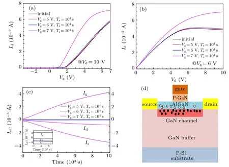
Fig.3. (a)Transfer characteristic curve;(b)output characteristic curve;(c)gate diode characteristic;(d)possible hole injection schematics.
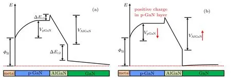
Fig.4. (a)Conduction band diagram of the metal/pGaN/AlGaN/GaN system at zero bias;(b)changes in conduction band diagram when stress-induced positive charges accumulate in p-GaN layer.
There have been explanations to this forward gate bias stress induced degradation. In Ref. [19] a donor-like trap generation in the P-GaN layer close to AlGaN is responsible for the localized leakage path. While Tallarico proposed in Ref. [20] a back to back connected junction of metal/PGaN schottky diode and PiN diode,where gate voltage mainly drops in the former and defects are generated in P-GaN close to the metal/P-GaN interface. While in our case,the progressive increasing of leakage is thought to be caused by hole injection from the top gate to the AlGaN,leading to a negative threshold voltage shift and increase in 2DEG concentration,as described in Fig.3(d). In the metal/pGaN/AlGaN/GaN system,by using the potential diagram shown in Fig.4(a),threshold voltage VTcan be described as follows:

where ΦBis the difference between the work function of the metal and the electron affinity of the semiconductor, VpGaNis the potential drop in p-GaN depletion layer due to the metal/pGaN Schottky barrier,?Ec1is the band offset between p-GaN and AlGaN, ?Ec2is the band offset between AlGaN and GaN,and VAlGaNis the potential drop in AlGaN layer due to the 2DEG response to the polarization electric field. We assumed that,positive charges will accumulated in the p-GaN layer as holes injection from the top gate to inner layer when the gate is biased at a large forward voltage. It is reasonable since the presence of defects related to Mg doping and the generation of defects due to the presence of a high electric field can lead to an increase of hole trap sites. As a mount of positive charges accumulate in p-GaN layer, the metal/pGaN Schottky barrier height is equivalent to be reduced,which induce a negative threshold voltage shift as described in Eq.(1).Another effect is that the positive charges in p-GaN/AlGaN interface could induce increased electrons in AlGaN/GaN interface, leading a larger potential drop VAlGaN, which also make a negative threshold voltage shift as described in Eq.(1).
In addition, the time when the fastest degradation happens is specified in Fig.5. When stressed at Vg=7 V,in the first 100-s duration there is not any degradation;While in the durations of 100 s–1000 s and 1000 s–10000 s, the threshold voltage shifts about 0.2 V and 1.5 V,respectively,as shown in Fig.5(c). This indicates that degradation mainly happens in the durations of 1000 s–10000 s;it can also be deduced in the Ig–Vgcurve at different time intervials, see Fig.5(d), where large gate degradation leakage current happens only in the durations of 1000 s–10000 s.
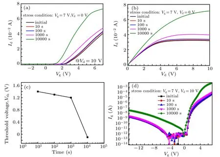
Fig.5. (a) Transfer characteristic curve; (b) output characteristic curve; (c) threshold voltage versus stress time; (d) gate diode characteristic; all at different durations in the 104-s forward gate stress.
3.3. Negative gate bias
Reverse gate bias stress was also performed, to our surprise, the degradation described in Ref. [18] did not occur in our case, even at an extremely high negative gate bias of?50 V, which is much higher than the “critical voltage” in Ref. [18]. This insensitive property under reverse gate bias stress may benefit from the high qualified GaN buffer, corresponding to the drain voltage stress experiment. By the way,this also guarantees a large gate swing in the negative direction. Figure 6 depicts the main I–V characteristic before and after reverse gate bias stresses.
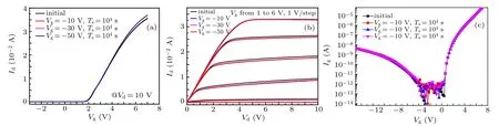
Fig.6. (a)Transfer characteristic curve;(b)output characteristic curve;(c)gate diode characteristic,all before and after reverse gate bias stresses.
4. Conclusion and perspectives
The reliability of normally-off p-GaN gate AlGaN/GaN high-electron mobility transistor was evaluated extensively by drain voltage stress,forward and reverse gate stresses. The insensitivity of the DUT under high drain stress and reverse gate stresses indicate a high qualified GaN buffer and SiN surface passivation layer, however, degradation is found severe when summoned to forward gate stress at Vg=7 V, and becomes more significant with increasing stressing time. We assume this degradation is mainly caused by hole accumulation in the AlGaN barrier close to p-GaN/AlGaN interface at high electric field. While this degradation mainly occurs in the gate to source region,process technology may be refined and controlled in this region to manufacture high voltage, more reliable normally-off p-GaN gate AlGaN/GaN high-electron mobility transistor.
猜你喜歡
Chinese Physics B(2023年10期)2023-11-02 08:40:00
趣味(數(shù)學(xué))(2022年5期)2022-07-29 03:24:28
趣味(數(shù)學(xué))(2022年5期)2022-07-29 03:24:24
趣味(數(shù)學(xué))(2022年5期)2022-07-29 03:24:18
趣味(數(shù)學(xué))(2022年6期)2022-07-29 03:03:22
趣味(數(shù)學(xué))(2022年6期)2022-07-29 03:03:22
Chinese Physics B(2022年5期)2022-05-16 07:10:54
語數(shù)外學(xué)習(xí)·高中版上旬(2020年8期)2020-09-10 07:22:44
Communications in Theoretical Physics(2018年6期)2018-06-15 07:32:40
女士(2015年3期)2015-07-05 01:11:32

- Chinese Physics B的其它文章
- Quantum annealing for semi-supervised learning
- Taking tomographic measurements for photonic qubits 88 ns before they are created*
- First principles study of behavior of helium at Fe(110)–graphene interface?
- Instability of single-walled carbon nanotubes conveying Jeffrey fluid?
- Relationship between manifold smoothness and adversarial vulnerability in deep learning with local errors?
- Weak-focused acoustic vortex generated by a focused ring array of planar transducers and its application in large-scale rotational object manipulation?