
Effect of Sb composition on the band alignment of InAs/GaAsSb quantum dots*
2021-01-21 02:08:34GuangzeLu陸光澤ZunrenLv呂尊仁ZhongkaiZhang張中愷XiaoguangYang楊曉光andTaoYang楊濤
Chinese Physics B 2021年1期
Guangze Lu(陸光澤), Zunren Lv(呂尊仁), Zhongkai Zhang(張中愷),Xiaoguang Yang(楊曉光),?, and Tao Yang(楊濤)
1Key Laboratory of Semiconductor Materials Science,Institute of Semiconductors,Chinese Academy of Sciences,Beijing 100083,China
2Center of Materials Science and Optoelectronics Engineering,University of Chinese Academy of Sciences,Beijing 100049,China
Keywords: quantum dots,type-II band alignment,intermediate-band solar cell,molecular beam epitaxy
1. Introduction
As zero-dimension active gain materials, quantum dots(QDs)have been widely used in opto-electronic devices,such as communication lasers,[1,2]silicon photonics transmitters,[3]infrared detectors,[4,5]Q-bit emitters,[6]and intermediateband solar cells (IBSC).[7,8]To enhance the performance of IBSCs and infrared detectors, QDs with long carrier lifetime are highly desirable.[9]During last decade,InAs/GaAsSb QDs have attracted much interest because of its variable band alignment. A rapid decrease in the valence-band energy of GaAsSb cap layer with increasing Sb composition result in a type-II band alignment.[10]The spatial separation of electron–hole pairs in InAs/GaAsSb QDs with a type-II band alignment is expected to lead to reduced carrier recombination and increased carrier lifetime. Recently, some groups have reported IBSCs based on InAs/GaAsSb QDs with a type-II band alignment.[11,12]Contrary to theoretical expectations,all these devices show dropped open-circuit voltages and efficiencies compared with reference IBSCs based on InAs/GaAs QDs with a type-I band alignment. One of the reasons is the low carrier lifetime of the fabricated InAs/GaAsSb QDs.As reported so far, the carrier lifetime of InAs/GaAsSb QDs with a type-II band alignment are generally a few nanoseconds.[13,14]The high density of strain-induced dislocations inside the InAs/GaAsSb QDs caused a minority carrier recombination, leading the open-circuit voltage degradation. Another reason is that the band alignment of InAs/GaAsSb QDs needs to be further revealed.Most studies consider that there is only one carrier recombination process in InAs/GaAsSb QDs,which lead to a much simplified band structure.[15]
In this work, InAs/GaAsSb QDs with different Sb components in the cap layers have been grown using molecular beam epitaxy (MBE). The effect of Sb component on the band alignment and related carrier recombination processes of InAs/GaAsSb QDs have been studied. Photoluminescence(PL) and power-dependent PL measurements have been used to characterize the properties of the InAs/GaAsSb QDs. The results reveal that the band alignment of InAs/GaAsSb QDs is strongly effected by Sb component. When the Sb component is 14%,InAs/GaAs0.86Sb0.14QDs show a complex band structure,with a type-I and a type-II carrier recombination processes respectively. It indicates that the QDs is in the critical state of transformation between type-I and type-II.As the Sb component is increased to 22%,InAs/GaAs0.78Sb0.22QDs exhibit three carrier recombination processes, and all of them are from the type-II band alignments. To obtain further insight into the dynamic mechanism,the time-resolved PL measurements have also been tested. The results show that the carrier lifetime of InAs/GaAs0.78Sb0.22QDs reaches 16.86 ns,which is about 8-times longer than that of InAs/GaAs0.86Sb0.14QDs (2.07 ns). The remarkably increased carrier lifetime offers a substantial potential for the enhancement of novel optoelectronic applications.
2. Experiment
Samples used in the study were grown using a Riber Compact-21 MBE system. As schematically illustrated in Fig. 1(a), all of samples were grown on n+-GaAs (100) substrates. After the substrate deoxidation,a 500-nm GaAs buffer layer was first deposited at 580?C.Then the temperature was cooled down to 470?C, and an inner layer of InAs QDs was grown with a coverage of 3.0 monolayers. After a 30-second pause, the inner InAs QDs were covered by a 5-nm lowtemperature cap layer which was grown at 470?C.The components of low-temperature cap layers were In0.18Ga0.82As for sample A that was a reference, GaAs0.86Sb0.14for sample B, and GaAs0.78Sb0.22for sample C, respectively. Then the temperature was increased to 600?C, and a 95-nm hightemperature GaAs cap layer was subsequently grown. Finally,the temperature was cooled down to 470?C,and surface InAs QDs which were used for atomic force microscopy (AFM)test were grown under the same growth conditions as the inner InAs QDs. Figure 1(b) shows a typical AFM image of the surface InAs QDs. The density of QDs is approximately 6×1010cm-2. It is found that the InAs QDs have a good uniformity,their average height and diameter are 3 nm and 35 nm,respectively.
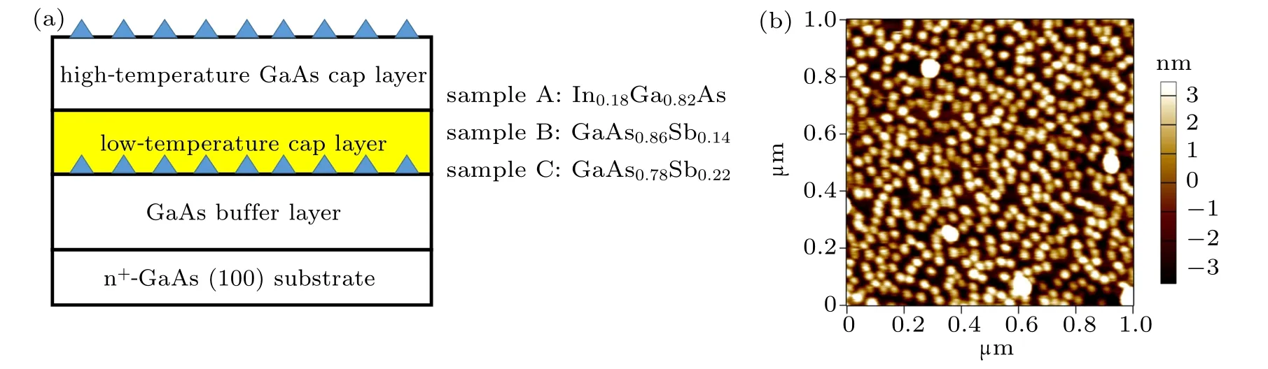
Fig.1. (a)Schematic structure of samples with different low-temperature cap layers,(b)AFM image of the surface InAs QDs.
3. Results and discussion
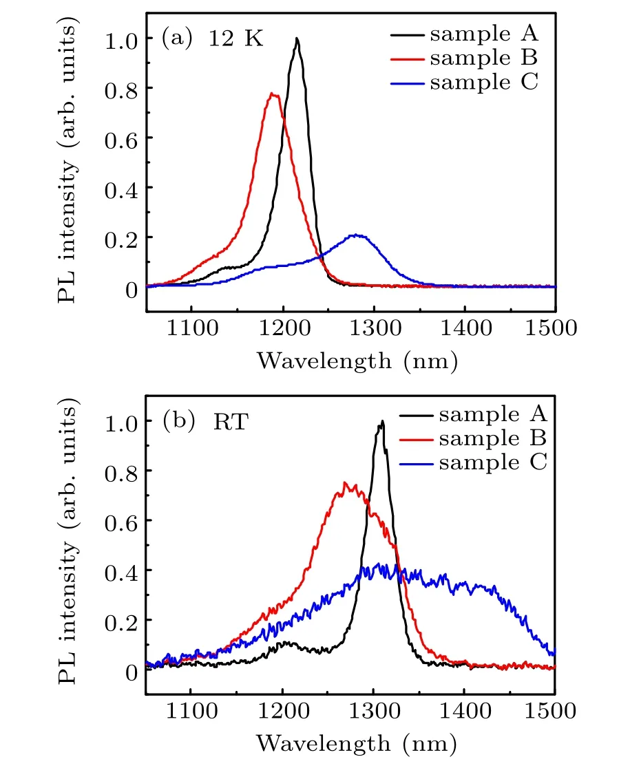
Fig.2. PL spectra of samples measured at(a)12 K and(b)RT.
Figure 2 shows the PL spectra of samples measured at a low temperature of 12 K and room temperature (RT). At 12 K, sample A exhibits a sharp emission peak at 1215 nm.The full-width at half-maximum(FWHM)of the peak is only 29.5 meV,which implies a quite good uniformity of the InAs QDs. The emission peak of sample B locates at 1188 nm and has an FWHM of about 48 meV. The increased spectral linewidth for sample B could be related to the segregation of Sb atoms in the GaAsSb cap layer. Sample C shows in turn a significant red-shift emission peak at 1280 nm. At RT, the FWHM of emission peak of sample A is still a small value,but the emission peaks of sample B and sample C obviously broaden. Because of the electron thermal excitation,more energy levels in QDs can be filled in at RT, which could cause a wider Gaussian-peak. Furthermore,sample C shows a fairly wide emission peak,with the longest wavelength emission occurring at 1500 nm.
To further investigate the band structures of samples,power-dependent PL measurements were performed at 12 K.The excitation powers were varied from 5 mW to 500 mW.The power-dependent PL spectra of samples as well as their peak energies as a function of excitation powers are shown in Fig.3. With increasing excitation power,the peak intensity of the peak 1 for sample A rapidly saturates and the peak intensity of the peak 2 correspondingly significantly increases,as shown in Fig.3(a).Meanwhile,the peak energies of the two peaks for sample A remain unchanged as the excitation power increases.It indicates that the band alignment of InAs/In0.18Ga0.82As quantum dots for sample A is typically type-I.It is found from Fig. 3(b), as the excitation power increases, the peak energy of the peak 1 for sample B is nearly unchanged. However,the peak energy of the peak 2 exhibits a linear increase with the excitation power,which indicates that the carrier recombination processes related to the peak 2 is type-II.Moreover, for sample C,all of the peaks show a significant and linear blue-shift with the excitation power, as shown in Fig. 3(c), which implies a pure type-II band alignment of the InAs/GaAs0.78Sb0.22QDs.[16,17]
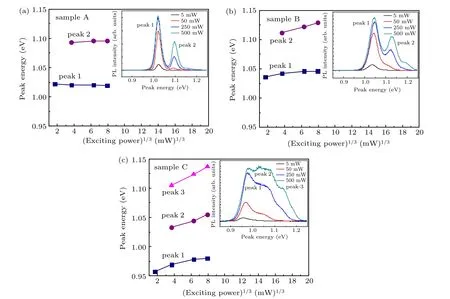
Fig.3. The peak energies as a function of the excitation powers for samples measured at 12 K.The insets show the power-dependent PL spectra of samples with increased excitation power from 5 mW to 500 mW.
To further confirm the band alignment of samples, timeresolved PL decay traces were measured at 10 K. The test system were performed using a 532-nm semiconductor laser as the excitation source. The signal was collected using a diffraction-limited confocal microscope objective and measured by a time correlated single photon counting (TCSPC)device. Using an exponential function
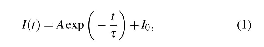
the time constant (τ) of the QDs related to each peak for samples was extracted. Figure 4 shows the time-resolved PL decay traces of the emission peaks for samples and their schematic illustrations of the corresponding carrier recombination processes. For the InAs/In0.18Ga0.82As QDs of sample A, τ related to the peak 1 and peak 2 is 1.02 ns and 0.48 ns,which indicate that the peak 1 and peak 2 resulted from the(E0→H0) and (E1→H1) transitions, respectively. For the InAs/GaAs0.86Sb0.14QDs of sample B, τ related to peak 1 and peak 2 is 1.04 ns and 2.07 ns. Due to strong intermixing between As atoms and Sb atoms,an As–Sb alloy layer will form between InAs QDs and GaAsSb cap layers.When the Sb component is low,the As-Sb alloy layer will localize the holes into the InAs and GaAsSb valence band respectively.[18]Combined with the power-dependent PL measurement,peak 1 and peak 2 were the emission peaks of(E0→H0)and(E0→H′0)transitions. For InAs/GaAs0.78Sb0.22QDs of sample C, τ related to three peaks is 5.50 ns, 2.87 ns, and 16.86 ns, respectively. When the Sb component is high,all holes are localized in GaAsSb valence band.[19]Also combined with the powerdependent PL measurement, the peak 1 and peak 2 originate from the (E0→H0) and (E1→H1) transitions, the peak 3 is resulted from(EGaAs→H0)transition. Clearly, the spatial separation of the electrons and holes for InAs/GaAsSb QDs with type-II band alignment results in a much longer lifetime.Based on the QDs with long carrier lifetime, a high conversion efficiency of intermediate-band QD solar cells can be expected.
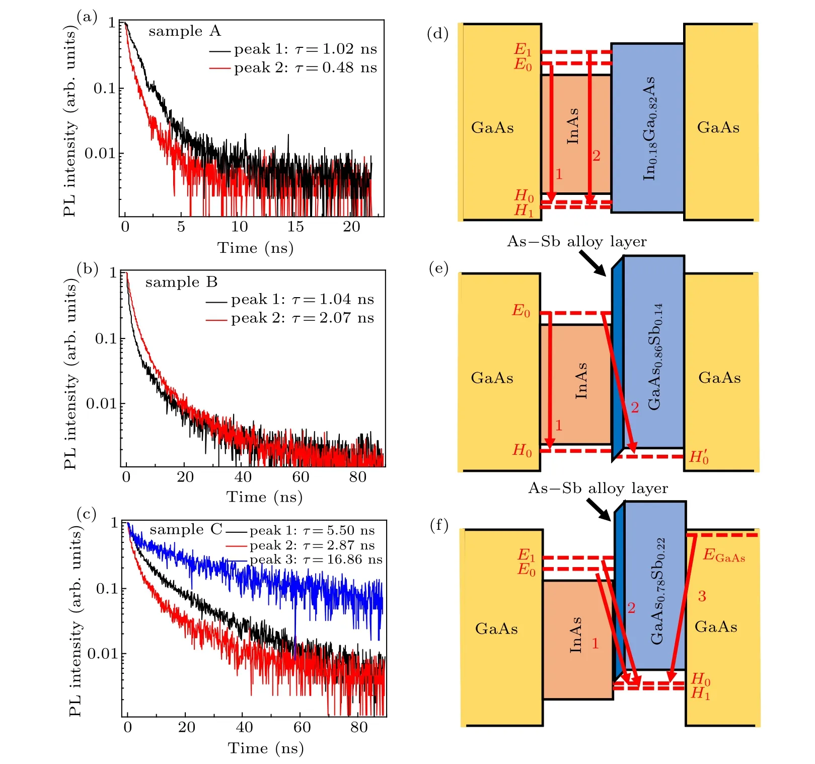
Fig.4. (a)–(c)Time-resolved PL spectra of simples and the time constant of each peak. (d)–(f)The band structure scheme of simples and the carrier recombination processes related to each peaks.
4. Conclusions
The band structures of InAs/GaAsSb QDs with different Sb component have been comparatively studied by PL, power-dependent PL, and time-resolved PL measurements. InAs/GaAs0.86Sb0.14QDs have a complex band alignment, with type-I and type-II carrier recombination processes. InAs/GaAs0.78Sb0.22QDs have a pure type-II band alignment with three type-II carrier recombination processes. Because the spatial separation of the electrons and holes, InAs/GaAsSb QDs with type-II band alignment have a much longer carrier lifetime. It is found that the carrier lifetime of InAs/GaAs0.78Sb0.22QDs reaches 16.86 ns,which is about 8-times and 16-times longer than ones of InAs/GaAs0.86Sb0.14QDs and InAs/In0.18Ga0.82As QDs, respectively. The results obtained here show helpful for understanding of the band alignment and carrier recombination processes of InAs/GaAsSb QDs with different Sb components,and the potential to develop high conversion-efficiency IBSCs.
猜你喜歡
ELLE世界時裝之苑(2023年10期)2023-10-10 23:30:46
當(dāng)代黨員(2022年9期)2022-05-20 13:35:21
當(dāng)代黨員(2022年9期)2022-05-20 13:35:21
Chinese Physics B(2021年12期)2021-12-22 06:41:28
Acta Mathematica Scientia(English Series)(2020年6期)2021-01-07 06:44:22
海峽姐妹(2019年7期)2019-07-26 00:50:56
Journal of Oceanology and Limnology(2018年3期)2018-07-11 01:58:26
小資CHIC!ELEGANCE(2018年20期)2018-07-06 02:31:46
中國化妝品(2018年3期)2018-06-28 06:21:08
小雪花·成長指南(2017年6期)2017-07-03 18:16:59

- Chinese Physics B的其它文章
- Numerical simulation on ionic wind in circular channels*
- Interaction properties of solitons for a couple of nonlinear evolution equations
- Enhancement of multiatom non-classical correlations and quantum state transfer in atom–cavity–fiber system*
- Protein–protein docking with interface residue restraints*
- Effect of interaction between loop bases and ions on stability of G-quadruplex DNA*
- Retrieval of multiple scattering contrast from x-ray analyzer-based imaging*