
High-performance waveguide-integrated Ge/Si avalanche photodetector with small contact angle between selectively epitaxial growth Ge and Si layers?
2019-06-18 05:42:26XiaoQianDu杜小倩ChongLi李沖BenLi黎奔NanWang王楠YueZhao趙越FanYang楊帆KaiYu余凱LinZhou周琳XiuLiLi李秀麗BuWenCheng成步文andChunLaiXue薛春來
Chinese Physics B 2019年6期
Xiao-Qian Du(杜小倩),Chong Li(李沖),Ben Li(黎奔),Nan Wang(王楠),Yue Zhao(趙越),Fan Yang(楊帆),Kai Yu(余凱),Lin Zhou(周琳),Xiu-Li Li(李秀麗),,Bu-Wen Cheng(成步文),and Chun-Lai Xue(薛春來),?
1State Key Laboratory on Integrated Optoelectronics,Institute of Semiconductors,Chinese Academy of Sciences,Beijing 100083,China
2Center of Materials Science and Optoelectronics Engineering,University of Chinese Academy of Sciences,Beijing 100049,China
3Institute of Electronic Information and Control Engineering,Beijing University of Technology,Beijing 100124,China
Keywords:waveguides,photodetectors,waveguide devices
1.Introduction
Avalanche photodetectors(APDs)have been utilized for a wide range of commercial,military,and research applications.[1]The APD receivers that are available on the market are typically made of III-V compound semiconductors,whose gain bandwidth products are limited(typically in the range of 100 GHz-150 GHz)by their low absorption coefficient at telecom wavelengths[2]and low ionization coefficient of multiplication layer.[3]Therefore,most of these photodetectors have been studied.[4-6]In recent years,Ge/Si separate absorption,charge,and multiplication(SACM)APDs have become promising candidates for future digital communication because they combine ef ficient optical absorption of Ge at communication wavelengths with outstanding electron multiplication properties of Si.[7-9]Moreover,waveguide coupling structure overcomes the trade-off between absorption effi ciency and bandwidth by a long horizontal optical path to absorb most of the photons and a short vertical carrier collection path to minimize carrier transit-time.[10-12]
However,the waveguide(WG)coupling Ge/Si SACMAPD suffers from the low coupling efficiency problem.The first waveguide-coupled Ge/Si APD exhibits a primary responsivity of 0.6 A/W at 1550 nm(QE=48%)with a coupling length of 70μm,[13]which is almost eight times longer than traditional p-i-n Ge/Si waveguide photodetector under the same responsivity.[14]The major restriction of the responsivity is the coupling efficiency between Ge/Si avalanche photodetector and single-mode Si waveguide.The thickness of Si single-mode WG is 0.22μm,yet the thickness of the Si layer of a Ge/Si SACM-APD is the sum of the thickness of Si contact layer and Si multiplication layer,determined by the avalanche multiplication process and multiplication factor of the devices.Normally,high sensitivity Ge/Si APD requires Si thickness of 1μm.[15,16]Obviously,there is a huge mismatchof thickness between SiWGand Si layer of Ge/Si APD,resulting in a source model overlap and reduced coupling efficiency.
Therefore,many approaches have been proposed to improve the coupling efficiency of Ge/Si WG-SACM-APD.Directly evanescent coupling waveguide Ge/Si SACM-APD of 30-μm-diameter by selective Ge and Si growth has achieved a primary responsivity of 0.8 A/W.[17]Then,fringing electric field was utilized to collect the photon-generated carriers and reduce the thickness of Si layer of the APDs.[18]However,the fringing electric field can hardly be controlled arti ficially,which means that excess noise,transmit time,and optical-generation carrier collection efficiency of the APDs are all unpredictable.[19]Moreover,vertical Ge absorption,lateral Si charge,and multiplication con figuration were proposed to keep evanescent coupling by single mode waveguide.[20]Unfortunately,the best experimental characteristics are a bandwidth of 9.81 GHz and a responsivity of 0.8 A/W at 1550 nm with 15.9μm device length,[21,22]far below expectation.The most promising candidate was step-coupler approach,which is based on the vertical multimode interference(MMI)and could theoretically achieve > 70%absorption with 10-μm-long Ge absorption region at 1550 nm using a step coupler.[23]Several step-coupler Ge/Si WG-SACM-APDs were continuously fabricated,researched,and reported.Unfortunately,satisfactory coupling efficiency has not yet been achieved.[24-26]
In this paper,we demonstrate two step-coupler lengths(1.5μm and 3.0μm)for waveguide-integrated Ge/Si SACMAPDs.The responsivity of APDs with step-coupler length of 3.0μm was 0.51 A/W at-6 V,21%higher than that of 1.5μm,which agrees well with simulated results.The maximal responsivity with step length of 3.0μm is 38.4 A/W.The maximum 3-dB bandwidth of the device is 15.3 GHz.The device with a length of 20μm and a step length of 3.0μm shows high performance with gain-bandwidth products of 376 GHz.
2.Device fabrication
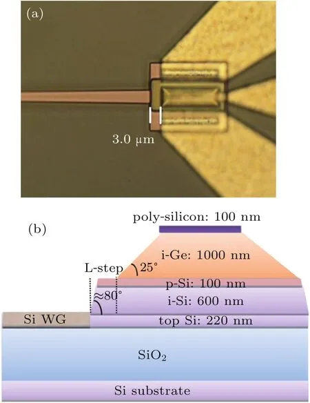
Fig.1.(a)The top view of the fabricated device with the step-coupler length of 3.0μm and the Ge length of 20μm;(b)the schematic crosssectional view of the waveguide Ge/Si SACM-APD.
Figures 1(a)and 1(b)schematically shows the top and cross-sectional views of the step-coupler waveguide Ge/Si APD,respectively.The starting silicon-on-insulator(SOI)wafer has~ 220-nm-thick p+-type top Si layer and ~2-μmthick buried oxide.After the channel waveguide and detector region definition,a 600-nm-thick Si layer is selectively epitaxial grown on the contact Si region by an ultra-high vacuum chemical vapor deposition(UHVCVD)reactor,followed by the p-type charge layer formation by implanting boron.Subsequently,another oxide window is opened and a 1-μmthick selectively epitaxial growth(SEG)Ge is grown by the same UHVCVD epitaxy reactor.The top and sidewalls of the epi-Ge are then covered with 100 nm of amorphous Si(a-Si)for passivation.The a-Si layer is implanted with a high dose of boron ions.The dopants are activated at 750°C for 3 minutes in the atmosphere of nitrogen to form a good p-type ohmic contact.The fabrication process is completed after the formation of aluminum interconnects.
3.Coupling efficiency and responsivity
The responsivity of a waveguide-integrated avalanche photodetector is limited by combination of(i)the absorption efficiency of Ge layer and(ii)the coupling efficiency betweenSi waveguide and Ge/Si APD. Three-dimensional finitedifference-time-domain (3D-FDTD)simulation is employed to investigate the absorption in the step coupler structures.The refractive indexes of Ge,Si,and SiO2at 1550 nm are 4.0,3.48,and 1.46,respectively.An absorption coefficient of 3000/cm at 1550 nm is used.[27]Figure 2(a)shows the simulated absorption versus the length of the step-coupler(L-step),and the maximal coupling efficiency is 58%at the step length of 3.0μm.The coupling efficiency is 48%at the step length of 1.5μm.The simulated absorption efficiency of APDs with step-coupler length of 3.0μm was 20.8%higher than 1.5μm.
Meanwhile,the responsivity of the fabricated devices with a step-coupler length of 3.0μm and 1.5μm at different voltage is measured,as shown in Fig.2(b).The responsivity of 3.0μm and 1.5μm is,respectively,0.51 A/W and 0.42 A/W at-6 V bias without multiplication.Obviously,there is a 21%improvement of the 3.0μm-step-coupler-length devices compared with 1.5-μm devices,which is in perfect agreement with the simulation results.Furthermore,if the collection efficiency is supposed to be 90%,the absorption efficiency of the fabricated devices is 45.3%and 37.3%,respectively,lower than the simulation results,which may result from the two contact angels around selectively epitaxial growth Ge and Si layers.Speci fically,the main absorption occurs around the 25°contact angle between the Ge and Si layers,as shown in Fig.2(c).However,the drift electric field around the smaller contact angleis much lower than the intermediate section of the absorber,which lowers the real absorption efficiency significantly.[10]Moreover,the 80°contact angle between epitaxial growth Si layer and top Si would have effect on the optical field distribution in the step-coupler and further lower the coupling efficiency.
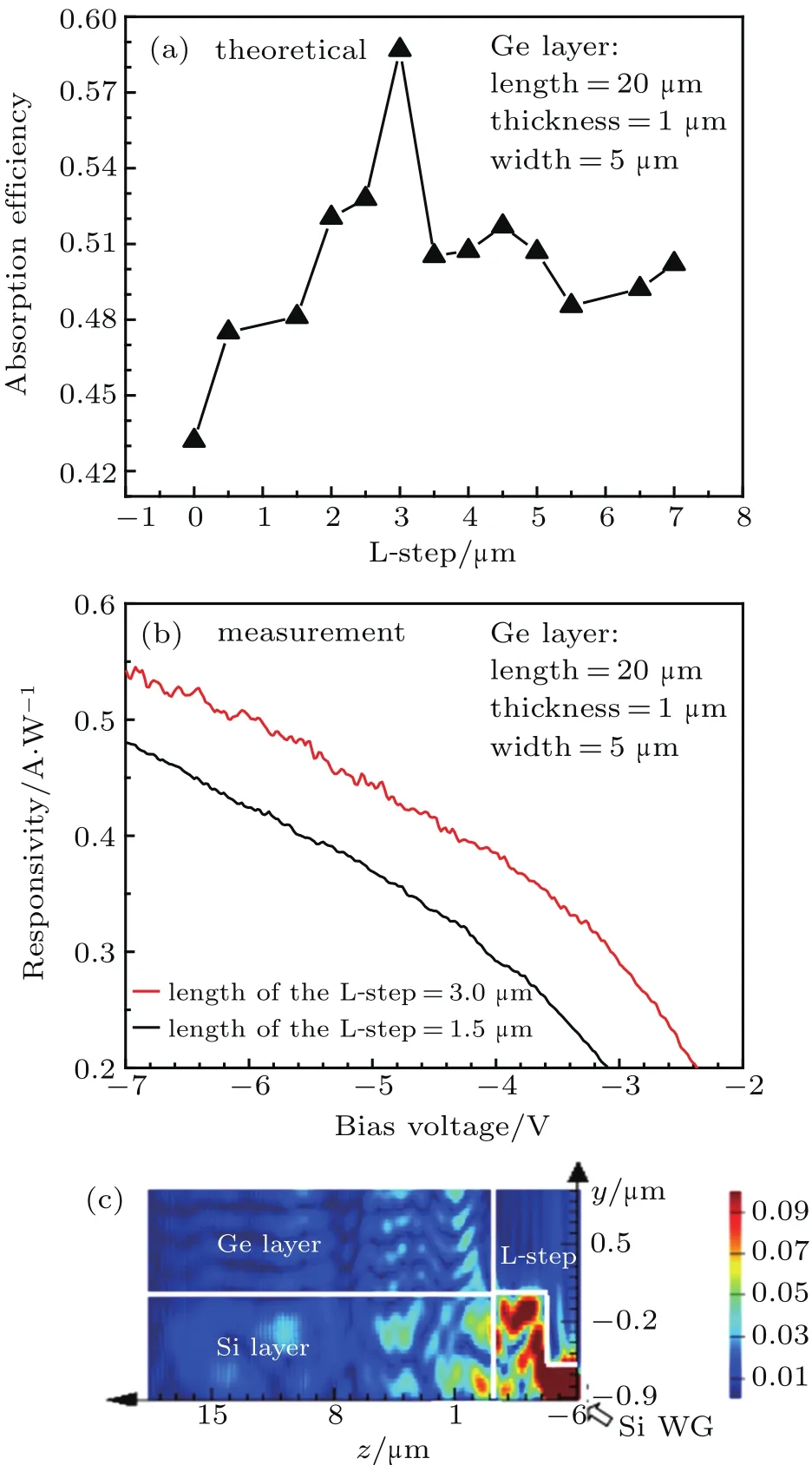
Fig.2.(a)Simulated absorption for the step-coupler structure with Ge length of 20μm,thickness of 1μm,and width of 5μm as a function of L-step;(b)responsivity of the two step-coupler(length of 1.5μm and 3.0μm)devices versus different bias voltages;(c)cross-sectional view of electric field intensity E in a structure of step-coupler length of 3.0μm.
4.Multiplication factor MMM and bandwidth(BW)
The performance of avalanche photodetectors is mostly characterized by multiplication factor M,3-dB bandwidth,and gain-bandwidth products.Figure 3(a)shows the room temperature dark and optical current-voltage characteristics of the fabricated APDs with 3.0-μm-step-coupler-length(APD-3.0)and 1.5-μm-length(APD-1.5)step-coupler by an Agilent B1500 semiconductor device analyzer.For the photocurrent measurement,a 1.55-μm wavelength,4.64-μW optical signal is coupled from a single-mode lensed fiber.The photocurrent rapidly rises in the bias voltage range of 0 V to-4 V.Breakdown voltages Vb,de fined at a dark current of 100μA,are found to be-24.7 V(APD-3.0)and-25.7 V(APD-1.5).Our APDs exhibit a reasonably low value of 4.1μA(APD-3.0)and 5.6μA(APD-1.5)at 90%of the breakdown voltage.The small difference of the breakdown voltages and dark currents is due to the series resistance effect of the two devices.The series resistance of APD-1.5 is larger than APD-3.0,which is estimated from the semi-log plot of the forward I-V curve,as shown in Fig.3(a).The multiplication factors M of two step-coupler devices with different Ge lengths are shown in Fig.3(b).The M factors of the APDs are calculated by the responsivity of waveguide-integrated Ge/Si p-i-i-p detector(~0.76 A/W).APD-3.0 has a maximum responsivity of 38.4 A/W.The maximum M factor is 50 for the APD-3.0 with 20-μm-Ge-length.However,the maximum M is only 17 for the APD-1.5 with the same Ge length,indicating that the fabricated APD might suffer from an unexpected breakdown,such as edge breakdown.
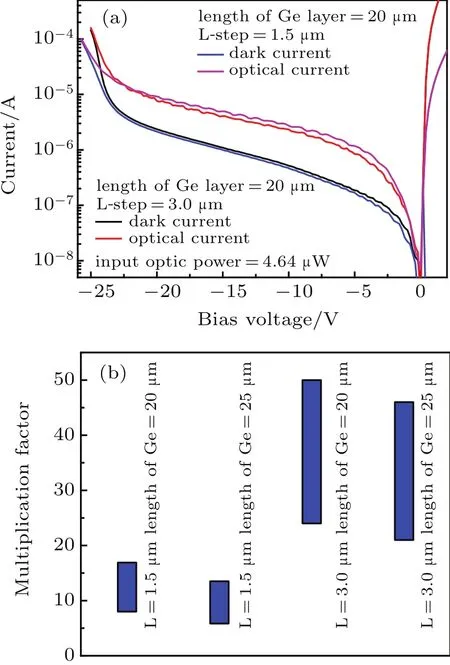
Fig.3.(a)The darkcurrent and photocurrent characteristics versusvoltage of the 3.0-μm-length and 1.5-μm-length step-coupler Ge/Si APDs with 20-μm-Ge-length.(b)The M scattergram of four types of devices.
A lightwave-component-analyzer(LCA)system is utilized to characterize the dynamic performance of the device by measuring the frequency responses of the scattering(S)parameters.This system is composed of a network analyzer(Anritsu 37397C),a well-calibrated electro-optics(EO)modulator(MOD)operated at 1550-nm optical wavelengths,and a tunable semiconductor laser operated at 1550 nm as the light source for this system.The adopted E-OMOD is provided by Sumitomo,which shows a 3-dB bandwidth of 40 GHz under 1550-nm optical pumping wavelength.Figures 5(a)and 5(b)show the measured bias-dependent O-E frequency responses of structures APD-3.0 and APD-1.5,respectively.The 3-dB bandwidths of APD-3.0 and APD-1.5 are 15.3 GHz and 14.7 GHz at-15 V,respectively,which are very close,due to the similar vertical structure.The maximum gain-bandwidth product of 376 GHz is obtained when the gain is 25.1 and bandwidth of 15 GHz of APD-3.0.The bandwidth of APD detector is mainly dominated by the carrier transit-time-limited bandwidth ftand resistor-capacitor(RC)bandwidth fRCin the active region.To improve the RC-limited 3-dB frequency response,both of the capacitance and the resistance should be minimized.Low capacitance,which is always limited below sub-pF in the other studies(references),can be achieved by careful design of the pro files of depleted layer.The parasitic impedance is related to the ohmic contact and electrical design,which can be improved by reducing ohmic contact resistance and optimizing the passivation process.

Fig.4.Normalized RF response for(a)APD-3.0 and(b)APD-1.5 with 20-μm-length structure at reverse bias of 15 V,20 V,23 V,and 25 V.
5.Conclusions
In conclusion,step-coupler waveguide-integrated Ge/Si SACM avalanche photodetector is fabricated by a complementarymetal-oxide-semiconductor (CMOS)-compatible process on 8-inch SOI platform.The responsivity of the APD with a 3.0-μm-step-coupler-length is 0.51 A/W,21%higher than that of 1.5μm,which matches well with the simulated absorption by FDTD method.The maximum values of 3-dB-bandwidth and multiplication gain factor for the APD are 15.3 GHz and 50,respectively.The APD with 20-μm-length structure and 3.0-μm-length step achieves high performance with a gainbandwidth product up to 376 GHz.
- Chinese Physics B的其它文章
- Theoretical study of overstretching DNA-RNA hybrid duplex?
- influence of carbon coating on the electrochemical performance of SiO@C/graphite composite anode materials?
- Spin glassy behavior and large exchange bias effect in cubic perovskite Ba0.8Sr0.2FeO3-δ?
- Aging mechanism of GaN-based yellow LEDs with V-pits?
- Magnetotransport properties of graphene layers decorated with colloid quantum dots?
- Temperature-dependent subband mobility characteristics in n-doped silicon junctionless nanowire transistor?