
Band engineering of valleytronics WSe2-MoS2 heterostructures via stacking form,magnetic moment and thickness
2023-11-02 08:38:40YanweiWu吳彥瑋ZongyuanZhang張宗源LiangMa馬亮TaoLiu劉濤NingHao郝寧Wengang呂文剛MingshengLong龍明生andLeiShan單磊
Chinese Physics B 2023年10期
Yanwei Wu(吳彥瑋), Zongyuan Zhang(張宗源), Liang Ma(馬亮), Tao Liu(劉濤),Ning Hao(郝寧), Wengang L¨u(呂文剛), Mingsheng Long(龍明生), and Lei Shan(單磊),§
1Information Materials and Intelligent Sensing Laboratory of Anhui Province,Key Laboratory of Structure and Functional Regulation of Hybrid Materials of Ministry of Education,Institutes of Physical Science and Information Technology,Anhui University,Hefei 230601,China
2State Key Laboratory of Metastable Materials Science&Technology and Key Laboratory for Microstructural Material Physics of Hebei Province,School of Science,Yanshan University,Qinhuangdao 066004,China
3Anhui Province Key Laboratory of Condensed Matter Physics at Extreme Conditions,High Magnetic Field Laboratory,Chinese Academy of Sciences,Hefei 230031,China
4Beijing National center for Condensed Matter Physics,Beijing Key Laboratory for Nanomaterials and Nanodevices,Institute of Physics,Chinese Academy of Sciences,Beijing 100190,China
Keywords: valleytronics,thickness,stacking,magnetic moment
1.Introduction
In the past years, two-dimensional (2D) materials have attracted many researchers’ interest due to their particular magnetic,[1,2]electronic and optical properties.[3-7]For transition metal dichalcogenide (TMD) systems, when thinned down to monolayer,lots of new physical properties were discovered,such as the direct bandgap,[8,9]non-centrosymmetric crystal structure, and valley-contrasting optical selection rule.[10-13]
It is known that transition metal dichalcogenides(TMDs)with a honeycomb lattice such asMX2(M= Mo/W;X=S/Se)consist of hexagonalX-M-Xcovalently bonded quasi-2D structures.In monolayer situation, TMDs exhibit a direct bandgap which is in the visible frequency range.Owing to the inversion symmetry breaking and strong spin-orbit coupling, monolayer TMDs exhibit two inequivalent spin-valley polarized band edges atKand-Kpoints at the corners of the hexagonal Brillouin zone (BZ).As a new degree of freedom(DOF)beside spin and charge,circularly polarized light,[11-14]magnetic fields,[15,16]strain,[17]spin-polarized current[18]and magnetic proximity effect[19-21]can be used in valley regulation.Such attractive interaction between spin and valley pseudospin makes monolayer TMDs an ideal platform for spin manipulations,valley physics and valleytronics applications.
As a common method, the construction of heterostructures[22-24]is widely used in the tuning of band structure in 2D materials’ applications.Former studies of vertical stacking van der Waals heterostructures have been successfully carried out.Applications and related theories have demonstrated the efficient interlayer electron transfer and tunable layer population of electrons and holes.[25-29]However,regulation of electronic structures of 2D materials is still critical and challenging.Many methods, such as dichalcogenides doped with magnetic transition metal atoms,[30-33]applying electric field,[34]adjusting temperature,[35]and strain regulation,[34,36,37]have been reported.In the method of temperature adjusting, the range of the bandgap tuning is very small (~10-1meV/K).As for strain regulation, large shape variable is hard to achieve although the bandgap change is very considerable.Since spin-orbit coupling is not considered,methods such as applying external electron field and doping magnetic transition metal atom dichalcogenides[30-32]are independent of spin valley physics.
In this study, we have investigated the electronic structures of WSe2-MoS2heterostructures in different stacking form and thickness.We combine the monolayer WSe2with monolayer(ML),bilayer(BL)and three layers(TL)2H-MoS2in structure construction.In order to find the effect of the magnetic moment on band gap engineering,we have added az-axis magnetic moment to different stacking WSe2-MoS2heterobilayers.Results suggest that stacking form,thickness and magnetization are effective in the regulation of valleys’ light absorption in WSe2-MoS2heterostructures,providing new ideas of photoelectric applications in this valleytronics system.In addition,Ref.[38]has investigated the breaking of valley degeneracy in MoSe2monolayer by an out-plane magnetic field up to 6.7 T at 4.2 K,providing the feasibility of our ideas.
2.Methods
We perform all calculations by employing the Viennaab-initiosimulation package (VASP)[39-41]within the framework of the projector augmented wave (PAW) method.The generalized gradient approximation (GGA) parameters by Perdew-Burke-Ernzerhof (PBE)[42]are used as the exchange-correlations, van der Waals correction (DFT-D2)method[43]is accounted to describe the van der Waals interactions.To investigate the different stacking type, we adopt 2×2 unit cells for the structure construction.In geometry optimizing,we adopt 25 °A vacuums slabs forMX2(M=W/Mo,X=S/Se) monolayers while 20 °A vacuum slabs for WSe2-MoS2heterobilayers.The cutoff energy of the plane-wave basis is set to 400 eV.A 10-5eV electronic iteration convergence criterion with a 0.01 eV/°A force tolerance is set for all calculations for structure relaxing.For ML WSe2-TL MoS2systems, we calculate these heterostructures by using real space projectors to reduce the computation.In addition,we use Gamma-centered 11×11×1 Monkhorst-Packk-point sampling grid for geometry optimization and 13×13×1 for static self-consistency.Magnetic moment (0.03-0.15μB) is added inz-direction to the supercell of all heterostructures.Spin-orbit coupling(SOC)is considered in all systems.
3.Results and discussion
3.1.Thickness and stacking forms of WSe2-MoS2 heterostructures
It is known that the monolayerMX2is in the form ofXM-Xand consists a hexagonal of Mo/W layer sandwiched between two S/Se layers.The structure of 2H-MoS2is symmetrical in a hexagon,with two layers as a period,and forms a triangular prism coordination with Mo atom as the center(shown in Fig.1(a)).
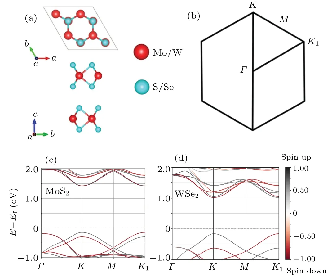
Fig.1.(a) Top and side views of 2H-MX2 (M =Mo/W, X =S/Se),(b) hexagonal Brillouin zone (BZ) and high symmetry points of 2D structure, (c) and (d) calculated band structures (with SOC) of monolayer MoS2 and WSe2.
We first consider the effect of different stacking on bandgap tuning of the heterostructures.As shown in Fig.2,we have divided these heterostructures into six groups,which are called I,II,III,IV,V and VI.At the interface of all structures in the same group, WSe2and MoS2have the same stacked interlayer.
We have performed a calculation of the electronic structures for different stacked WSe2-MoS2heterostructures to illustrate how the thickness affects the bandgap.Results are listed in Figs.3,S1 and S2.
As shown in Figs.3(a),S1 and S2,all stacking types have direct band gap and spin-valley polarization.In Fig.3(b),the CBMs are mainly contributed by Mo in the MoS2layer(s),while the VBMs are mainly contributed by W of the WSe2monolayer.Due to the degenerated CBM, the valley index(K/K1point)is determined by the stacking direction of monolayer WSe2,which is also indicated in Fig.S1(types I,III and V have the same valley index, while types II, IV, VI possess the other consistent index).Raising thickness of 2H-MoS2increases both band gap andK/K1points’CBM degeneracy.To illustrate the results more precisely,we summarize the results in Table 1.
As shown in Table 1,our results suggest that the bandgaps of monolayer MoS2and WSe2agree well with previous studies.[34,44,45]Compared with MoS2and WSe2monolayers, the construction of WSe2-MoS2heterobilayers reduces the bandgap with a maximum value of 1.308 eV.On this basis,the energy gap can be finely regulated by the layer thickness and stacking mode of the heterojunction.Increasing the thickness of 2H-MoS2raises the bandgap in all stacking forms.Besides, the effect of band gap regulation also depends on the stacking type.Such tuning ranges suggest that the thickness of 2H-MoS2in the constructions of MoS2-WSe2heterostructures has advantages in electronic devices (such as field effect transistors and photodetectors).On the other hand, due to the 2D properties, the MoS2-WSe2heterostructures’ particular optical and electrical properties have broad prospects in the fields of small-scale, high-performance optoelectronic and nano devices.In addition,the direct band gap also makes MoS2-WSe2heterostructures suitable for optical applications.
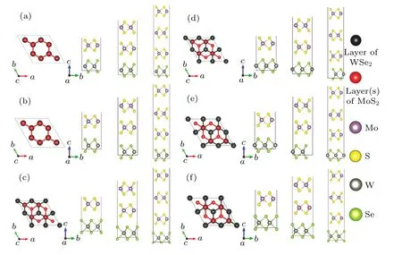
Fig.2.Top and side views of WSe2-MoS2 heterostructures atomic model with six different stacking forms: (a)-(f)I-VI form stacking.

Table 1.Calculated bandgaps (eV) of heterostructures composed of monolayer MoSe2 and different thickness of 2H-MoS2 in six stacking forms.
3.2.Band engineering via magnetic moment
To investigate the effect of thez-axis magnetic moment atK/K1points, thek·pmethod and DFT are both adopted.AtK/K1points,the Hamiltonian of all WSe2-MoS2heterobilayers described by thek·pmethod can be written as[14]
in whichτ=±1 is the valley index,athe lattice constant,tthe effective hopping integral,Δthe band gap, ?σthe Pauli matrices for two basis functions, ?sthe Pauli matrices for spin.The last term of Eq.(1) describes the SOC, where|2A| and|2B|deal with the spin split at conduction-band-edge and valenceband-edge (for monolayer MoS2and MoS2-WSe2heterobilayers,A=0).When considering an addedz-axis magnetic field,the Hamiltonian reads
Here,it should be noticed that the magnetic term is small and has not coupled with other terms.From which we can get the band edges atK/K1points:The first and third eigenvalues stand for the spin split in the conduction band edges while the second and fourth eigenvalues illustrate the spin split in the valence band edges.As mentioned above,the induced magnetic moment makes different band edges atK/K1points.In the situations ofA=0,CBMs have no difference atK/K1points with the rise of the magnetic moment, which still gives a direct bandgap.Generally speaking, the rising of magnetized term decreases the band gap.
Now, we have computed the WSe2-MoS2heterobilayers with magnetic moment(z-axis)in the range of 0-0.15μB(interval 0.03μB).We list the bandgaps of all situations in Table 2 and show the computed band structures of 0.03μB,0.06μB,0.09μB,0.12μBand 0.15μBin Figs.4 and S3.
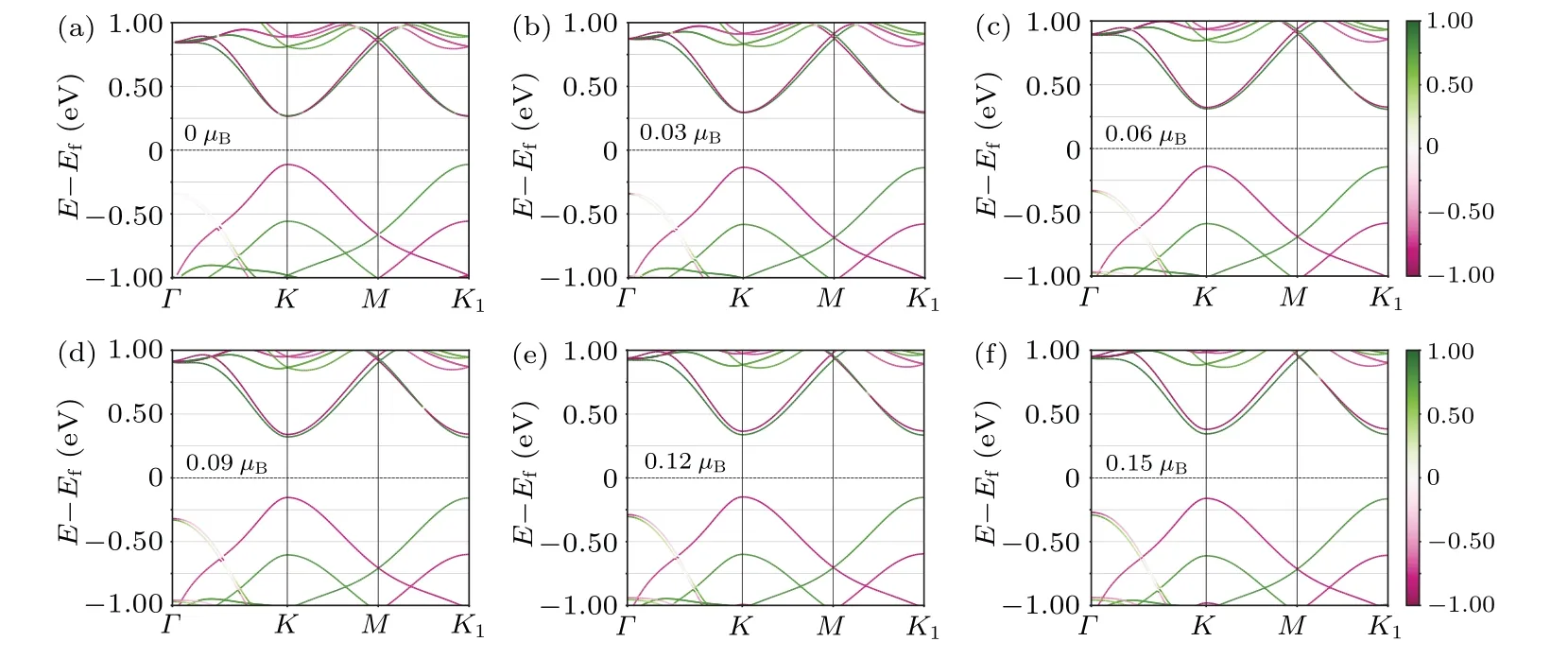
Fig.4.Calculated band structures of magnetized VI form stacked WSe2-MoS2 heterobilayers with magnetic moment of (a) 0.00 μB,(b)0.03μB,(c)0.06μB,(d)0.09μB,(e)0.12μB,(f)0.15μB.Green and red colors indicate the spin-up and spin-down polarization.

Table 2.Calculated bandgap (in eV) of I-VI stacking WSe2-MoS2 heterobilayers with magnetic moments(ranging from 0 to 0.15μB).
As the difference of band edges betweenKandK1points is small,we use the difference between CBM and VBM as the band gap.As listed in Table 2, in all kinds of stacking types,the bandgap increases with the enhancement of the magnetic moment.Moreover, the tuning effect of magnetic moment depends on the stacking type.With a magnetic moment of 0.15μB,more than 0.4 eV bandgap tuning appears in II-group stacking while I-group stacking only has a 0.159 eV bandgap regulation.For all six heterobilayers, the total free energies (without SOC) of I-VI type stackings are-181.189 eV,-180.845 eV,-181.110 eV,-181.166 eV,-180.859 eV,and-181.194 eV,respectively,in which types II and V have more advantages in the magnetized situations,they have similar total free energies(~-180.8 eV).The total free energies of another group containing types I, III, IV and VI are all close to-181.2 eV,and the tuning effects on the bandgap of these stacking types are relatively close.Furthermore, the increase of magnetic moment raises a difference in band edges atKandK1points,which is similar to the results of thek·pmethod.
Compared withMX2(M=Mo/W,X=S/Se) monolayers, the multilayer situations are more complex due to the interlayer coupling.In the typicalk·pmethod, the given systems are assumed to be fixed.In other words, the magnetic moments in this model should be very small to keep the system parameters(such as lattice constants and atom positions)unchanged which has negligible influence on the lattice.On the other hand,DFT calculations can consider larger magnetic moments due to full geometry optimization (coupling of the magnetic moment and the structure parameters).As a result,for a specific system, thek·pmethod is only applicable in a small range of magnetic moments,while the DFT calculation is suitable for a larger range of magnetic moment.
4.Conclusion and perspectives
In summary, we have performed a study of spin-valley polarization in six stackings of WSe2-MoS2heterostructures and magnetized bilayer systems by DFT.Calculations show thatMX2monolayers and all six different stackings of WSe2-MoS2heterostructures have direct-bandgap and valleytronics properties.Compared withMX2monolayers,the construction of WSe2-MoS2heterobilayers achieves significant bandgap reduction(maximum 1.308 eV).On this basis,the rising thickness of 2H-MoS2can further regulate the band gap which depends on the stacking form.Furthermore, we have investigated thez-axis magnetized WSe2-MoS2heterobilayers,bothk·pmethod and DFT demonstrate that thez-axis magnetic moment introduces different band edges atK/K1points.For relatively larger magnetic moment,the band gap changes significantly.Similar to the thickness of 2H-MoS2, the effect of the magnetic moment in band gap tuning also depends on the stacking type.As a result, the magnetic moment and thickness can be used as the further regulation means of stacking form to band engineering.Compared with previous studies,our methods are more effective and easier experimentally achieved.Our results suggest that WSe2-MoS2heterostructures are suitable platforms for spin-valley applications due to their tunable direct bandgaps and valleytronics properties.In addition, thickness, stacking form and induced magnetic moment give controllable methods in the optical absorption of 2D multilayers,we believe our calculations are suitable for applications in 2D spin-valley nanostructures.
Acknowledgements
Project supported by the National Natural Science Foundation of China (Grant Nos.61975224 and 12104004), the University Synergy Innovation Program of Anhui Province(Grant No.GXXT-2020-050), the Fund of Anhui Provincial Natural Science Foundation(Grant No.2008085MF206),New magnetoelectric materials and devices, the Recruitment Program for Leading Talent Team of Anhui Province 2020, State Key Laboratory of Luminescence and Applications (Grant No.SKLA-2021-03), and the Open Fund of Infrared and Low-Temperature Plasma Key Laboratory of Anhui Province(Grant No.IRKL2022KF03).
猜你喜歡
小學(xué)生學(xué)習(xí)指導(dǎo)·低年級(jí)(2023年9期)2023-11-08 03:04:01
小學(xué)生學(xué)習(xí)指導(dǎo)(低年級(jí))(2023年9期)2023-10-12 03:02:46
讀者(2023年15期)2023-08-22 09:13:59
Chinese Physics B(2022年10期)2022-10-26 09:46:26
黨政研究(2022年3期)2022-05-25 16:11:20
安徽文學(xué)(2021年12期)2021-12-21 00:42:52
金色年華(2017年7期)2017-06-21 09:27:52
中學(xué)生數(shù)理化·中考版(2015年12期)2015-09-10 07:22:44
作文周刊·小學(xué)五年級(jí)版(2014年1期)2014-08-16 08:19:10
意林(2014年5期)2014-04-10 15:40:53
- Chinese Physics B的其它文章
- Corrigendum to“Reactive oxygen species in plasma against E.coli cells survival rate”
- Dynamic decision and its complex dynamics analysis of low-carbon supply chain considering risk-aversion under carbon tax policy
- Fully relativistic many-body perturbation energies,transition properties,and lifetimes of lithium-like iron Fe XXIV
- Measurement of the relative neutron sensitivity curve of a LaBr3(Ce)scintillator based on the CSNS Back-n white neutron source
- Kinesin-microtubule interaction reveals the mechanism of kinesin-1 for discriminating the binding site on microtubule
- Multilevel optoelectronic hybrid memory based on N-doped Ge2Sb2Te5 film with low resistance drift and ultrafast speed