
Electronic properties and interfacial coupling in Pb islands on single-crystalline graphene
2022-03-12 07:44:46JingPengSong宋靖鵬andAngLi李昂
Chinese Physics B 2022年3期
關(guān)鍵詞:李昂
Jing-Peng Song(宋靖鵬) and Ang Li(李昂)
1State Key Laboratory of Functional Materials for Informatics,Shanghai Institute of Microsystem and Information Technology,Chinese Academy of Sciences,Shanghai 200050,China
2University of Chinese Academy of Sciences,Beijing 100049,China
Keywords: scanning tunneling microscopy,graphene,quantum well states,superconducting proximity effect
1. Introduction
As dimension decreases, exotic quantum phenomena emerge as a result of electronic confinement.[1]Electronelectron correlation is enhanced due to the reduced Coulomb shielding in a two-dimensional (2D) system. Meanwhile,the non-negligible surface and interfaces play an important role in determining the electronic properties of such lowdimensional materials/devices.[2-7]Graphene, as a representative of a real 2D system, has attracted tremendous interest in both fundamental research and industrial development in the past decades.[8]The unique band structure, the high electron mobility, the easy way to tune the carrier density,etc. make graphene an excellent platform for studying quantum phenomena at the 2D limit such as superconductivity.One strategy to introduce superconductivity into graphene is through the proximity effect by forming heterostructures with a superconductor. Substantial progress has been made in graphene-based superconductor devices[9-11]while previous studies are mostly macroscopic. A local investigation at an atomic level on the graphene-superconductor interface is still very challenging.[12,13]
In this work,Pb(111)nano-islands are successfully grown on the single-crystalline graphene/Ge(110) substrate. The electrons in Pb are weakly coupled to the graphene substrate, which endows the films with free-standing nature.We find no evidence for superconducting proximity effect in graphene. Alternatively, the well-protected electronic structure in Pb demonstrates well-defined quantum confinement which proves the feasibility of studying low-dimensional physics in graphene-based heterostructure system.
2. Experiment
The high-quality single-crystalline monolayer graphene was synthesized by chemical vapor deposition method on a Ge(110) substrate.[14]In this study, 100%-graphene coverage was chosen which corresponds to a growth time of about 100 min.
Prior to the deposition of Pb,the graphene samples were loaded into the ultra-high vacuum chamber (4×10-11mbar)(1 bar=105Pa) and degassed at 650°C for 1 h-2 h. After the graphene samples cooled down to room temperature,Pb was deposited with molecular beam epitaxy at a flux of 0.33 nm/min-0.50 nm/min for 4 min-6 min while the pressure was maintained below 2×10⁻⁹mbar. Afterwards, the Pb/graphene/Ge(110) samples were transferred to the STM chamber. All STM measurements were performed at 4.6 K with electrochemically etched tungsten tips. Each tip was conditioned and calibrated on a clean Cu(111)surface before use. Differential conductance(dI/dV)spectra were acquired by numerical derivative ofI-Vcurves (in the±2 V range)or standard lock-in technique (in the±10 mV range) with a 971 Hz/0.4 mV modulation.
3. Results and discussion
Figure 1(a) shows a typical topography of the graphene surface after lead deposition. Pb tends to form truncated triangle(occasionally hexagonal)islands randomly oriented. Step edges are rarely observed on these islands which are exclusively due to the steps in the Ge(110) substrate. Atomic resolution(Fig.1(b))on the islands reveals three-fold symmetry with an interatomic distance~3.6 °A, in agreement with that in the bulk Pb(111)plane(3.5 °A).[15]This confirms the facecentered cubic(fcc)crystal structure of Pb islands with(111)facet on the top. The heights of islands are thus measured in the unit of monolayer(ML)which corresponds to the Pb〈111〉interlayer distance(286 pm).[15]We investigate over 110 such islands and find their widths and heights to vary in a range of 10 nm-100 nm and 6 ML-37 ML,respectively. Instead of the amorphous wetting layer commonly observed in Pb films grown on Ag(111)and Si(111),[16,17]perfect graphene lattice and underlying Ge(110) surface can be resolved at different bias voltages(Figs.1(c)and 1(d))on the substrate away from the islands. This means that there is no continuous wetting layer formed on the graphene substrate before Pb islands start to grow.
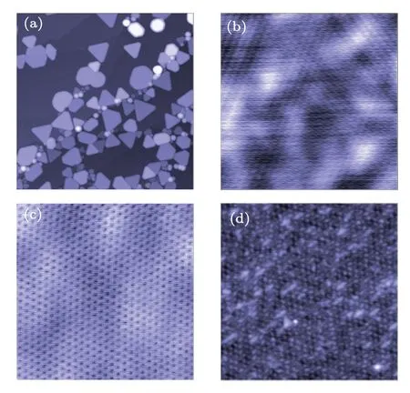
Fig.1. (a)Surface morphology of Pb islands on single-crystalline graphene(1000 nm×1000 nm,bias voltage Vb=2 V,tunneling current I=50 pA).(b)Atomic resolution on a Pb island(15 nm×15 nm,Vb=20 mV,I=300 pA).(c) Atomic resolution on single-crystalline graphene (6 nm×6 nm, Vb =20 mV,I=300 pA).(d)Surface morphology on single-crystalline graphene on Ge(110)(40 nm×40 nm,Vb=2 V,I=50 pA).
The statistics of Pb island thickness values is shown in Fig.2. The ratio of odd-to even-numbered layer thickness is about 15:4. In a previous STM work,[18]it is reported that the even-numbered layer thickness dominates in the lead islands on graphene/Ru. Probably this discrepancy originates from the distinct lattice symmetries in the substrate underneath the graphene. The Ge(110) orthorhombic instead of Ru(0001)hexagonal substrate might induce different stresses in the films, hence influencing the stability of Pb islands on graphene.
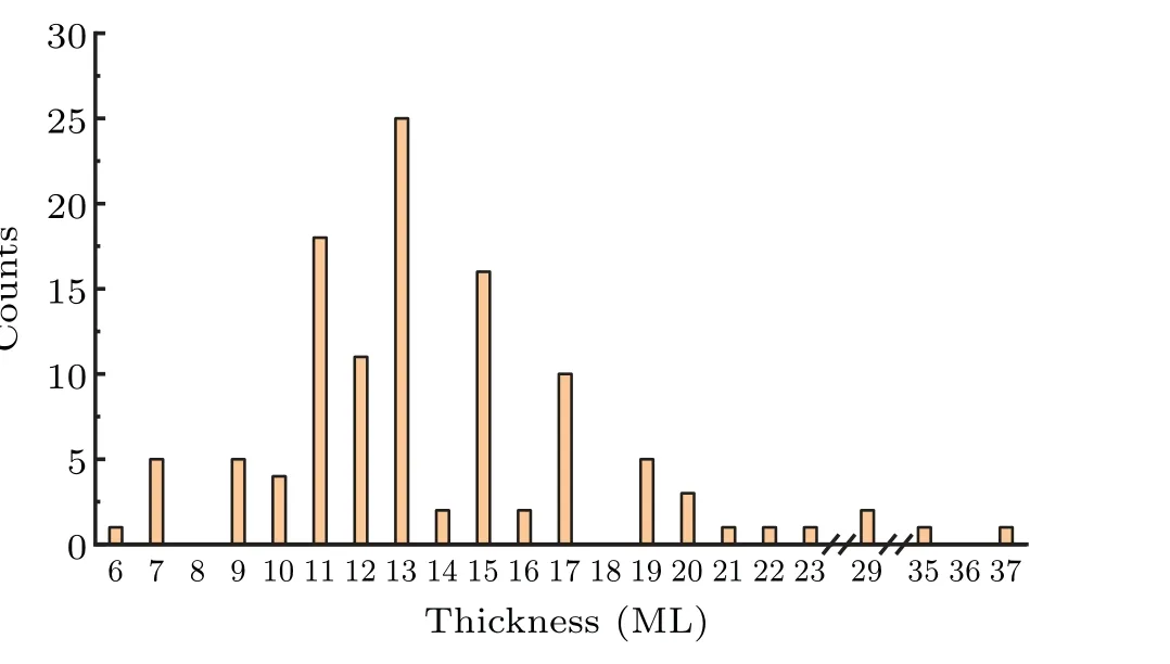
Fig.2. Statistics of island thickness values.
For the islands larger than 15 nm in width,[15]the quantum confinement plays a major part in determining their electronic structures. Itinerant electrons are confined in the vertical direction, resulting in discrete energy levels associated with the so-called quantum well states (QWSs).[19]We measure the dI/dVspectra(proportional to the electron density of states)in an energy range from-2 eV to 2 eV on Pb islands with different thickness values. In Fig.3(a),a series of dI/dVpeaks emerge on the empty state (positive bias) side, marking the discrete energy levels of QWS.The energy separation between the QWS peaks decreases as the thickness of island increases, which can be described by the phase accumulation model.[20]
According to an infinite-well model in a lead film,[19]
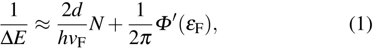
where ΔEis the energy separation between QWSs,dis the interlayer distance,Nis the number of layers,his the Planck constant,νFis the Fermi velocity, andΦ′(εF) is the energy derivative of the interface electronic phase shift at Fermi level. It can be seen that the inverse of the energy separation obeys a linear dependence on film thickness as demonstrated in Fig.3(b). The intercept at the thickness axis,which is 0.14 nm±0.05 nm (0.49±0.17 ML), tells the vertical distance over which free electrons are restrained in the metal film. It is quite different from a previous study on Pb/Si(111)
where a negative intercept(-3 ML)is observed. The nonnegative intercept indicates that the QWS electrons cannot penetrate into the graphene substrate. The poor electronic transparency at the Pb/graphene interface signifies a weak electronic coupling between graphene and the Pb islands. Serving as a blocking layer, the graphene further protects the QWSs from overlapping with the underlying germanium bands (our Ge(110) substrate is Ga-doped with partial gap~600 meV)which would otherwise lead to strong scattering that dramatically shortens the quasiparticle lifetime and reduces the electron confinement.[21]
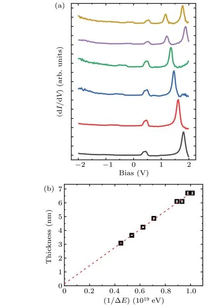
Fig. 3. (a) Quantum well states in dI/dV spectra for Pb islands of different thickness values. From bottom to top: 11, 13, 15, 17, 21, and 23 ML(Vb =2 V,I=1 nA).(b)Thickness versus 1/ΔE of Pb islands. Red curve is linear fit,yielding intercept+0.14 nm(0.49 ML).
The weak coupling across the Pb/graphene interface is further evidenced by the Pb electronic structure as revealed by the tunneling spectrum. Figure 4 shows such two spectra recorded on 13-ML- and 21-ML-thick islands. Splitting of QWS peaks around Fermi level(≤+0.5 V)and the subsequent narrowing into Lorentzian shape at higher energy values reveal a close resemblance to the spectral features found in Pb islands deposited on graphene/SiC, which are in good agreement with the density functional theory(DFT)-calculated band structure of a free-standing Pb(111)film.[15]The strong interaction with the substrate bulk states, on the contrary, will result in significant reduction in quasiparticle lifetime and hence smearing of QWS peaks at all energy values just like the case in Pb/Si(111).[22]Here passivated Ge(110) surface favors the growth of single-layer graphene under relatively mild conditions.[14]Two or more graphene layers, like the case on SiC substrate, would further weaken the interfacial coupling and even lower the mechanical stability of Pb films.[15]The graphene/Ge(110) provides excellent thermal, electronic and mechanical performances for the metal films.
Pb is a conventional superconductor with the bulk critical temperature~7 K. When in close proximity to a normal metal, superconductivity can be induced in the normal metal that decays over the superconducting coherence length(~80 nm for Pb[23]) at clean limit. High electronic transparency at the interface is pre-required for the establishment of superconducting proximity effect. Therefore proximity effect in graphene can be used to justify the electronic coupling between graphene and Pb overlayer. Figure 5(a)shows a typical Pb island. Its size is apparently larger than the Anderson limit(~10 nm)[2]and the presence of superconductivity is evidenced by the pairing gap in tunneling spectrum. The superconducting pairing gap is spatially homogeneous over a distance of 70 nm (Fig. 5(c)), proving the good quality of our films. Away from the islands, however, the superconducting spectral features (partially depleted density of states below 2 meV and broadened coherence peaks at finite temperature) are lost immediately in neighboring graphene substrate. As demonstrated in Figs.5(b)and 5(d), the line shape returns to the shape of the intrinsic graphene spectrum(green)at 4 °A away from the edge of island, which is the closest limit we can reach experimentally due to the tip geometry.Considering the relatively large coherence length in our Pb island (>70 nm) and the high quality of single-crystalline graphene,[14]we believe that the proximity effect is completely suppressed in the graphene substrate. Cooper pairs are blocked by the interface from leaking into graphene. The absence of proximity-induced superconductivity is consistent with the fact that QWSs are essentially confined in the lead film itself.
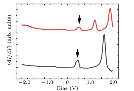
Fig.4. Plot of dI/dV versus bias of 13 ML(lower,black)and 21 ML(upper,red)island(Vb=2 V,I=1 nA),with arrows indicating splitting QWS peaks around 0.5 V.
Superconductivity in ultra-thin films has been extensively studied and the interfacial coupling is found to play an essential role in these low-dimensional systems.[2,5,24-26]In the Pb/graphene/Ge(110), the superconductivity develops in the Pb islands while the Cooper pairs can barely leak into graphene/Ge(110) substrate at a lateral distance as small as 4 °A. In this sense, the superconducting properties of Pb film are well protected. This is important for smaller(thinner)superconducting devices fabricated on this type of substrates,otherwise perceptible degradations will happen.
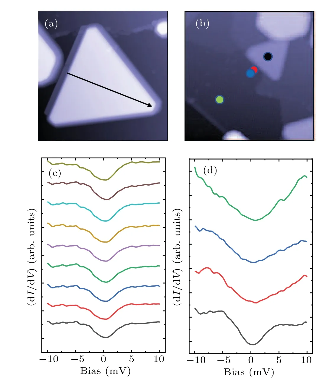
Fig. 5. (a) A 11-ML-thick typical Pb island on graphene/Ge(110). (b)Another Pb island, on and close to which the spectra are measured(180 nm×180 nm)as shown in panel(d). (c) dI/dV spectra recorded along the 70-nm-long arrow in panel(a)(Vb=10 mV,I=1 nA).(d)From bottom to top: representative dI/dV spectra measured on Pb (black), graphene at 0.4(red),0.6(blue),and 50 nm(green)away from the edge of Pb island as marked in panel(b)(Vb=10 mV,I=1 nA).
4. Conclusions and perspectives
In this work,Pb(111)islands grown on single-crystalline graphene/Ge(110) substrate show well isolated electronic behaviors. Electron confinement in the normal direction is restrained in the Pb islands without penetration into graphene. The spectroscopic features of QWSs are consistent with the band structure of a free-standing Pb(111)film.[15]The weak Pb/graphene interface coupling is further supported by the absence of superconducting proximity effect in graphene. Therefore it is concluded that the Pb(111) islands on graphene/Ge(110)are free-standing in nature,showing very weak electronic coupling to the substrate. The graphene/Ge(110)substrate provides an ideal support to maintain the intrinsic properties of thin films for studying exotic quantum phenomena at 2D limit.
Acknowledgements
We are grateful to Xiaowen Han and Zengfeng Di for providing graphene samples.
Project supported by the Science Foundation of the Science and Technology Commission of Shanghai Municipality,China(Grant No.18ZR1447300).
猜你喜歡
派出所工作(2024年8期)2024-12-31 00:00:00
老年人(2023年12期)2023-12-20 15:44:39
包裝工程(2022年9期)2022-05-13 13:03:10
Chinese Physics B(2021年5期)2021-05-24 02:23:36
科學(xué)文化評論(2021年4期)2021-04-24 21:15:42
電子競技(2019年4期)2019-04-20 05:29:28
百家講壇(2016年5期)2016-09-28 19:02:56
人生與伴侶·共同關(guān)注(2015年3期)2015-09-22 09:23:20
岷峨詩稿(2014年3期)2014-11-15 04:13:24
做人與處世(2014年10期)2014-07-17 21:09:39
- Chinese Physics B的其它文章
- Surface modulation of halide perovskite films for efficient and stable solar cells
- Graphene-based heterojunction for enhanced photodetectors
- Lithium ion batteries cathode material: V2O5
- A review on 3d transition metal dilute magnetic REIn3 intermetallic compounds
- Charge transfer modification of inverted planar perovskite solar cells by NiOx/Sr:NiOx bilayer hole transport layer
- A low-cost invasive microwave ablation antenna with a directional heating pattern