
Origin of anomalous enhancement of the absorption coefficient in a PN junction?
2021-09-28 02:21:02XianshengTang唐先勝BaoanSun孫保安ChenYue岳琛XinxinLi李欣欣JunyangZhang張珺玚ZhenDeng鄧震ChunhuaDu杜春花WenxinWang王文新HaiqiangJia賈海強YangJiang江洋WeihuaWang汪衛(wèi)華andHongChen陳弘
Chinese Physics B 2021年9期
Xiansheng Tang(唐先勝),Baoan Sun(孫保安),Chen Yue(岳琛),Xinxin Li(李欣欣),Junyang Zhang(張珺玚),Zhen Deng(鄧震),Chunhua Du(杜春花),Wenxin Wang(王文新),5,Haiqiang Jia(賈海強),5,Yang Jiang(江洋),?,Weihua Wang(汪衛(wèi)華),and Hong Chen(陳弘),5,?
1Institute of Physics,Chinese Academy of Sciences,Beijing 100190,China
2Key Laboratory for Renewable Energy,Beijing Key Laboratory for New Energy Materials and Devices,Beijing National Laboratory for Condensed Matter Physics,Institute of Physics,Chinese Academy of Sciences,Beijing 100190,China
3University of Chinese Academy of Sciences,Beijing 100049,China
4Center of Material and Optoelectronics Engineering,University of Academy of Sciences,Beijing 100049,China
5Songshan Lake Material Laboratory,Dongguan 523808,China
Keywords:PN junction,absorption coefficient,non-equilibrium statistical model
1.Introduction
Since the photovoltaic effect[1]was discovered,semiconductor materials with the PN junction have been widely used in photoelectric devices,such as solar cells[2–4]and photodetectors.[5–7]One of the main factors that needs to be considered in device design and preparation is the absorption coefficient,α,of the material.[8,9]αplays a significant role in selecting proper semiconductor materials,designing and analyzing photoelectric devices.[10,11]From the past knowledge,αis proportional to the transition probability and the density of states available for transition.[12]In general,αis a constant for a particular material at a corresponding wavelength.The calculations of absorption coefficients for a wide wavelength range have been well documented in the literature.[13–16]Many methods were also used to acquire absorption coefficients,including measuring the transmission spectrum,measuring permittivity,[14]and measuring photoluminescence and photothermal deflection spectroscopy.[17]These data of measurements are consistent with theoretical calculations.Doping and voltage application can changeα,[18–20]but the influence is small.
Recent experiments in GaAs material[21]and Si material[22]systems showed that when an intrinsic layer is inserted in the depletion region of the PN junction,forming a PIN structure,the absorption coefficient of this intrinsic layer can be enhanced significantly.[21,22]Furthermore,different thicknesses of this intrinsic layer have different absorption coefficients.The absorption coefficient of intrinsic GaAs and Si materials in a PIN structure can be respectively enhanced to 105cm?1and 104cm?1,an order of magnitude higher than the commonly used value.This enhanced absorption cannot be explained by the established theory.[12]The absorption process involves the transport process of photo-generated carriers,which should be a non-equilibrium process,and the photo-generated carriers will affect each other except for the interactions with phonons.The Brownian movement also involves the motion of many carriers,which can be solved by the stochastic equation theory in the non-equilibrium condition.It provides us with ideas to solve the problem.In this paper,we provide a general theoretical interpretation of the phenomenon of anomalous enhancement of the absorption coefficient based on the non-equilibrium statistical theory of carriers.We also analyzed the phenomenon by comparing the time scale of the relaxation process and transport process with statistical theory.The competition between the transport and relaxation process leads to an increase in the absorption coefficient.The theory can predict the experimental data well,helping us to understand the carrier transport in the PN junction and give new thoughts to design solar cells and photodetectors.
2.Method and discussion
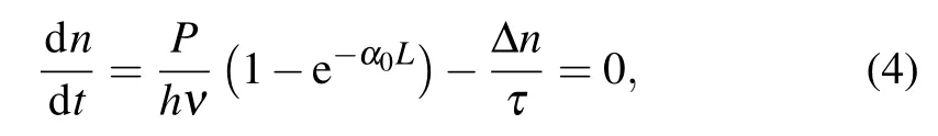
Before analyzing the transport of carriers in the intrinsic layer(named sample A)in the PIN structure,a reference sample shown in Fig.1 with a separate intrinsic layer(named sample B)was introduced.
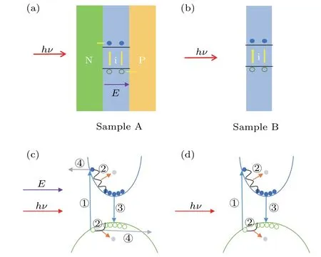
Fig.1.The green area represents the N layer,the yellow area represents the P layer,and the blue area represents the I layer.The blue solid spheres represent electrons,and the green hollow spheres represent holes.The quantity is meaningless.The blue line represents the conduction band,and the green line represents the valence band.(a)Sample A is a PIN structure,an intrinsic layer sandwiched by P-type layer and N-type layer.(b)Sample B is a separate intrinsic layer.(c)For sample A,there are four processes of photogenerated carriers:excitation,relaxation,recombination,and drift.(d)For sample B,there are three processes of photo-generated carriers:excitation,relaxation,and recombination.
When the system of sample A was in a stable state,photogenerated carriers would go through four processes,including excitation,relaxation,recombination,and drift.For simplicity,the relaxation process can be equivalent to the recombination process because the relaxation time is far less than the recombination.On the other hand,there is an assumption that photo-generated carriers start waiting for recombination once generated.When the number of non-equilibrium carriers is steady,the rate of changing of carriers should be zero.So,the generation rate is equal to the recombination rate plus the drift rate[23]

For sample B,when the system is stable,photo-generated carriers would go through three processes,which are excitation,relaxation,and recombination.Similarly,the process of relaxation can be equivalent to the process of recombination.The number of non-equilibrium carriers is steady,and the rate of changing is also zero,so the generation rate is equal to the recombination rate[23,24]

By combining Eq.(2)with Eq.(4),we get Now the velocity distribution W(v)is going to be analyzed.Photo-generated carriers belong to non-equilibrium carriers,and the motion of a large number of photo-generated carriers is similar to Brownian motion,so we can use the random theory,[24]Fokker–Planck theory.The carriers can be regarded as free electrons without an electric field.In the case of an electric field,it is in a non-equilibrium state.The electrons interact with each other,scattered by the crystal lattice,which can be considered as the viscous resistance.The quantitative analysis of electron interaction is complex.It can therefore be regarded as random noise.First,the Langevin equation is used to describe the dynamics of a free carrier without an electronic field[24]
where f=?γv is viscous resistance which describes the scattering of carriers,andγis the coefficient of viscosity.m?is the effective mass of carriers.Γ(t)is the random force exerted on one carrier at a given moment,indicating the influence of other carriers.Γ(t)has the following characteristics〈Γ(t)〉=0,〈Γ(t)Γ(t′)〉=qδ(t?t′),and q=(2γkT)/(m?2).k is the Boltzmann constant.T is the temperature.By solving equation(1),we know that,which is the velocity relaxation equation.So,γ=m?/τ,andτis the momentum relaxation time.
Similarly,the Langevin equation is used to describe the carriers in an electric field[24]
where F=eE is the electric field force on the carrier,and other parameters are the same as those in Eq.(1).As we know,the Fokker–Planck equation has the following form:[24]
where D1and D2are Kramers–Moyal expansion coefficients,and they can be obtained by combining with the Langevin equation(2).Their specific representation is as follows:D1=(F+f)/(m?),D2=q/2.Now we can get the exact form of the Fokker–Planck equation.When the system is in a steady state,dW(v,t)/dt=0.By solving the second-order homogeneous differential equation,the expression of W(v,t)is obtained as[24]
From Eq.(10)we know that the velocity distribution of carriers in the electric field can be described as the Boltzmann distribution,which still includes the basic pattern of the Boltzmann distribution.In some situations,we can use the Boltzmann distribution approximately to describe the velocity distribution.From Eq.(10),we can get the ratio of carriers at a different velocity,which is helpful for us to analyze the carrier transport further.
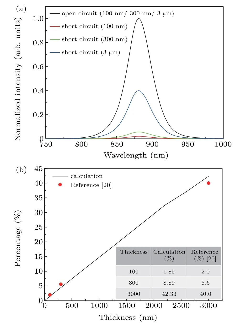
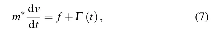
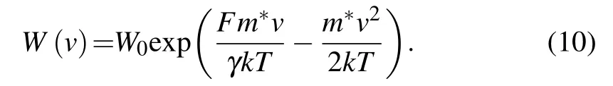
Fig.2.(a)Comparison of normalized fitting data of fluorescence intensities in open circuit and short circuit cases with different intrinsic layer thicknesses.The original experimental data comes from Ref.[20].(b)The proportion of carriers involved in the recombination varies with the thickness of the intrinsic layer in the PN junction based on GaAs material.The black line and the red dots are the calculation and the experimental data,respectively.

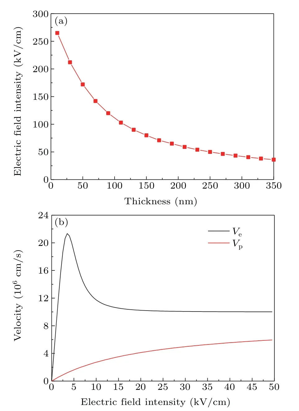
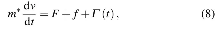
Fig.3.(a)The electric field intensity varies with an intrinsic layer thickness of PIN structure.(b)The velocity of electron and hole varies with electric field intensity in GaAs.
Figure 3(a)shows that the electric field intensity varies with the intrinsic layer thickness of the PIN structure,and it was obtained by simulation through Crosslight.Figure 3(b)shows the velocity of electron and hole varies with electric field intensity that was obtained by equation.[23]As can be seen from Figs.3(a)and 3(b),when the intrinsic layer thickness is less than 350 nm,the electric field intensity is strong enough to accelerate the carriers,including holes and electrons,to saturation speed.For GaAs,the saturation speed of the electron and the hole is 107cm/s and 6×106cm/s,respectively,as shown in Fig.3(b).Based on the above discussion,the absorption coefficient is related to the transport velocity.It is necessary to confirm the velocity of the carriers.In the actual situation,to maintain the neutral condition,the electron drift will decrease to match the hole drift,and the hole drift will increase to match the electron drift.For simplicity,the velocity of holes is taken as the transport velocity to calculate the absorption coefficient.

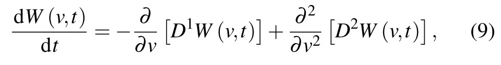
Fig.4.(a)The schematic diagram of the test system.(b)The fitting of experimental values and calculation values in GaAs material.The black line represents calculation values and the red dot represents experimental data.
The substitution of a constant by a variable absorption coefficient will tremendously impact the design of photoelectric devices based on the PN junction,such as photoelectric detectors and solar cells.First of all,due to the enhancement of the absorption coefficient,the reduced thickness of the absorption layer can favor saving epitaxy cost and guarantee higher crystal quality for heteroepitaxy with a huge lattice mismatch.For example,it is possible to use a thin in GaAs layer with a high In component grown on a GaAs substrate to make a photodetector at 1064 nm.Second,due to the enhancement of the absorption coefficient,the same amount of photocurrent can be generated from a thinner material,resulting in different carrier transport behavior.In the case of different intrinsic layer thicknesses,the proportion of photo-generated carriers involved in escape and recombination is different.The thinner the thickness,the greater the proportion of escaping.The greater the thickness,the greater the proportion of recombination.Reducing the thickness of the absorption layer does not reduce the photocurrent,but reduces the transit length of the carrier,thus reducing the transit time,making the state change faster,and improving the high frequency characteristics of the device.
A related theory of photoelectric devices needs to be reconsidered,such as fill factor in solar cells and the modulation frequency of the detectors.At last,we have successfully applied the stochastic equation theory related to Brownian motion to modeling the non-equilibrium carriers in the absorption process,which expands the application scope and provides ideas for solving related problems in the future.
3.Conclusion
The absorption coefficient varies with the thickness of the intrinsic layer in the PN junction,caused by the competition between recombination and drift for non-equilibrium carriers.When the absorption layer is thin enough to be of the order of hundreds of nanometers,the drift time is faster than the recombination time,which accelerates the absorption of light,leading to the enhancement of the absorption coefficient.With statistical theory,we proposed an equation to describe the relationship between absorption coefficient and material thickness.The equation fits the relevant experimental values well.This theory can help to explain the carrier transport in the PN junction and gives a new idea to design photoelectric devices.
猜你喜歡
幼兒100(2024年9期)2024-03-27 05:45:22
Chinese Physics B(2022年3期)2022-03-12 07:44:06
Chinese Physics B(2021年9期)2021-09-28 02:18:28
Chinese Physics B(2021年9期)2021-09-28 02:18:12
北極光(2020年1期)2020-07-24 09:03:54
故事會(2019年23期)2019-12-05 05:37:17
文學(xué)少年(小學(xué)版)(2019年5期)2019-07-26 14:25:45
心聲歌刊(2018年4期)2018-09-26 06:54:08
讀寫算·高年級(2017年7期)2017-08-09 00:48:30
學(xué)苑創(chuàng)造·A版(2016年4期)2016-04-16 18:29:21
- Chinese Physics B的其它文章
- Protection of isolated and active regions in AlGaN/GaN HEMTs using selective laser annealing?
- First-principles study of plasmons in doped graphene nanostructures?
- Probing thermal properties of vanadium dioxide thin films by time-domain thermoreflectance without metal film?
- An improved model of damage depth of shock-melted metal in microspall under triangular wave loading?
- Signal-to-noise ratio of Raman signal measured by multichannel detectors?
- Molecular dynamics study of coupled layer thickness and strain rate effect on tensile behaviors of Ti/Ni multilayered nanowires?