
Enhanced absorption process in the thin active region of GaAs based p–i–n structure?
2021-09-28 02:18:28ChenYue岳琛XianShengTang唐先勝YangFengLi李陽鋒WenQiWang王文奇XinXinLi李欣欣JunYangZhang張珺玚ZhenDeng鄧震ChunHuaDu杜春花HaiQiangJia賈海強(qiáng)WenXinWang王文新WeiLu陸衛(wèi)YangJiang江洋andHongChen陳弘
Chinese Physics B 2021年9期
關(guān)鍵詞:江洋
Chen Yue(岳琛),Xian-Sheng Tang(唐先勝),Yang-Feng Li(李陽鋒),Wen-Qi Wang(王文奇),Xin-Xin Li(李欣欣),Jun-Yang Zhang(張珺玚),Zhen Deng(鄧震),Chun-Hua Du(杜春花),Hai-Qiang Jia(賈海強(qiáng)),3,4,Wen-Xin Wang(王文新),3,4,Wei Lu(陸衛(wèi)),Yang Jiang(江洋),?,and Hong Chen(陳弘),3,4,?
1Key Laboratory for Renewable Energy,Beijing Key Laboratory for New Energy Materials and Devices,Beijing National Laboratory for Condensed Matter Physics,Institute of Physics,Chinese Academy of Sciences,Beijing 100190,China
2University of Academy of Sciences,Beijing 100049,China
3Center of Material and Optoelectronics Engineering,University of Academy of Sciences,Beijing 100049,China
4Songshan Lake Material Laboratory,Dongguan 523808,China
5State Key Laboratory for Infrared Physics,Shanghai Institute of Technical Physics,Chinese Academy of Sciences,Shanghai 200083,China
Keywords:photoelectric,p–n junction,absorption coefficient
1.Introduction
Strong interest of studies for optical absorption can be traced back to the discovery of photovoltaic effect in 1839.As the world is facing more and more serious energy shortage,solar cells become an important research direction.[1–4]On the other hand,with the coming of intelligence and information age,the development and design of new photodetectors and photoelectric sensors are in the ascendant.[5–8]Since the optical transition and absorption process are the physical bases of the above photoelectric devices,the study of absorption has attracted much attention of researchers.[9–13]
In the established theory of absorption process,the absorption coefficientαplays an important role,which is the basic macroscopic parameter in semiconductors manuals to characterize the microscopic optical transition.In 1962,the absorption coefficient was obtained by transmission measurements of Sturge.[14]Then,other researchers used the Kramers–Kronig analysis and detailed balance theory to calculate the absorption coefficient of GaAs based materials.[15–19]Today,the most widely used result is from Adachi which shows thatαof GaAs is 5.38×103cm?1at 1.42 eV at room temperature.[20]
Based on the traditional theory,the absorption coefficient of the direct transition can be calculated by the following formula:[21]
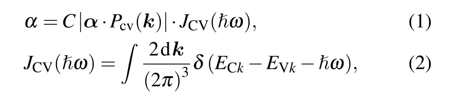
whereαis the unit vector of photon vibration,and Pcv(k)is momentum matrix element of the transition from the initial state to the final state,which is only related to initial and final wave functions.JCV(?ω)is called joint state density and obeys the relationship of JCV∝NC·NV.Theoretically,for a certain semiconductor material,the absorption coefficientαis only dependent on the wavelength of incident light.
However,recently there have been some experimental results showing anomalous enhancement of the absorption coefficient.[22–25]It is found that the absorption coefficient of the material between a p–n junction was enhanced up to an order higher than the commonly used value.These results of anomalous enhancement of the absorption indicate a new mechanism beyond the established theories.In response to the new discovery,unfortunately,there is no clear physical explanation for these phenomena in previous articles,even tentative discussions are rarely proposed.
In this paper,GaAs is chosen as the study object,since GaAs based optoelectronic materials have made great progress to get application in a lot of fields.[26–30]In our experiment,four GaAs based p–i–n structure samples with the depletion region of different thicknesses from 100 nm to 3μm were fabricated and tested for optical absorption from 1.4 eV to 3.1 eV.The enhancement of absorption was observed in this GaAs based p–i–n structure and a new theoretical model was put forward.
2.Experiments
Four GaAs based p–i–n structure films were grown by V80H molecular beam epitaxy(MBE)by V80H equipment on p-GaAs substrates.The contents of samples are shown in Fig.1,which consists of a p-GaAs substrate layer(used as the p-contact layer),a 500 nm p-GaAs layer with concentration of 4.5×1017cm?3,an intrinsic GaAs layer,a 150 nm n-GaAs layer with concentration of 5×1017cm?3and a 150nm n-GaAs contact layer.The thicknesses of the intrinsic GaAs layers which work as the active regions are 100 nm,300 nm,1μm and 3μm for the four samples,respectively.After the growth,the samples were fabricated to solar cells with the standard solar cells process.The contact pads are distributed on the opposite side of the samples.The light is incident through the n-GaAs contact layer and n-GaAs layer to get in the intrinsic layer.The size of each unit cell is 5.5×5.5 mm2.

Fig.1.The structure diagram of the samples.
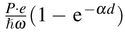
Then,photocurrent measurements were carried out for the four samples.A white light through a grating spectrometer was used as the excitation source,and the power distribution with the wavelength was measured by a standard power meter.The electrical properties were characterized by Keithley 4200-scs semiconductor parameter analyzer.To focus on the optical absorption,the following mentioned photocurrents in this paper were measured with no bias voltage.The relationship of the photocurrent and external quantum efficiency(EQE)could be given by the following formula:w
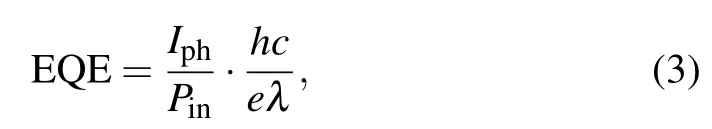
here Iphis the photocurrent,Pinis the power of the incident beam,h is Planck constant,c is the light velocity in the vacuum,e is the elementary charge andλis the wavelength of the incident beam.Results of the experiment and specific discussions are in the next section of this paper.
3.Results and discussion
With using hypothesis of complete ionization of impurities,the built-in electric field was simulated for all samples,as shown in Fig.2.
It demonstrates that the thinner depletion region has the higher intensity for the built-in electric field in the depletion region.The peaks at the p–i or n–i interface are caused by abrupt-junction due to the p–i or n–i contact.[31]There is no electric field in p or n regions,so only the carriers generated in the depletion region can drift to make contribution to the photocurrent,while in other regions unbalanced carriers can only do diffusion and most of them are consumed by recombination.
The photocurrents of four samples were given under the normalized 100μW incident light with continuous changed wavelength of 400–900 nm,which is shown in Fig.3(a).
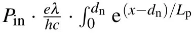

Fig.2.Simulated built-in electric field intensity for samples with different thickness for the active region.(a)Built-in field in 100 nm depletion region.(b)Built-in field in 300 nm depletion region.(c)Built-in field in 1μm depletion region.(d)Built-in field in 3μm depletion region.It demonstrates that there is no electric field in other regions except the depletion region.

Fig.3.Experimental results of four GaAs samples with different thicknesses of active region between the same p–n junction.(a)Photocurrents of four samples under the normalized 100μW incident light related to the wavelength of 400–900 nm.(b)Calculated photocurrents generated in the 300 nm n-typed region under the normalized 100μW incident light.(c)Comparison of the EQEs related to the wavelength of 400–900 nm obtained from the photocurrents of this study excluding those generated in the 300 nm n-typed region and the calculation by the absorption coefficients from Kramers–Kronig results of Adachi.[20]
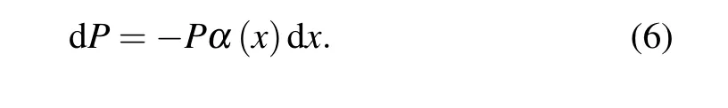
Absorption process is essentially the transition of electrons excited by incident photons.The excited electrons would recombine with the holes at the top of the valence band.However,within a p–n junction,because of the existence of built-in electric field,these unbalanced carriers are going to move in the depletion region.For a photogenerated carrier,the optical transition and absorption process could be demonstrated in following diagram,as shown in Fig.4.Firstly,the electrons are excited by incident photons from valence band to conduction band and this process takes time,t1.Then,some of these unbalanced carriers escape from the depletion region to external circuit forming photocurrent under the built-in field,which takes time,te.There are also some unbalanced carriers relaxing to the bottom of the conduction band due to the collision and scattering with lattice,which takes time,t2.These relaxed electrons finally recombine with holes in the valence band,which takes time,t3.Traditionally t2and t3are not considered in the absorption process and the absorption coefficient is independent of them.
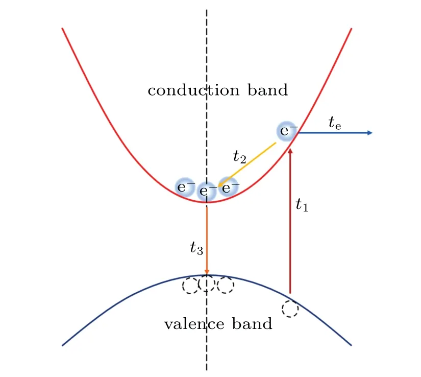
Fig.4.The diagram demonstrating the optical transition and absorption process in the active region in a p–i–n structure,which is based on the energy band in k-space.
According to the Pauli exclusion principle,when an electron is excited from the valence band to the conduction band,a state in the conduction band will be occupied and no other electrons could be excited to this state.Consequently,in the absorption process,an occupied excited state no longer contributes to the optical absorption.Each state switches between occupied and unoccupied state,but when the dynamic balance is achieved the total number of unoccupied excited states remains constant.Theoretically the excitation probability is equal to 1/t1,and analogously,the escaping probability can be described by 1/te.And teis related to the excitation position in the active region,which could be given by te(x)=x/vd.Here vdis the drift velocity under the built-in electric field,and x is the distance from the excitation position to the active region boundary with the n-type region.In the case without a p–n junction,the unoccupied state densities are NC0and NV0,respectively,and they are both proportional to 1/t1.When the active region is within a p–n junction,the unbalanced carriers can escape from the depletion region driven by the builtin field.The additional escaping path greatly accelerates the carriers leaving the occupied states,which will increase NC0and NV0to NCand NV.The additional part of the unoccupied state densities is proportional to 1/te,and NCand NVcan be acquired as the following formulas:
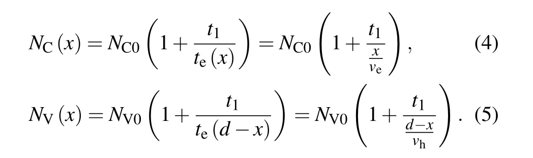
In the formulas,veand vhare the drift velocities of carriers in the built-in electric field in the active region of the conduction band and valence band,respectively.The drift velocity vdis given by vd=μEinand the mobilityμis regarded as 200 cm2/(V·s)and 1500 cm2/(V·s)for holes and electrons,respectively.[32,33]Einis from the simulation results shown in Fig.2.Considering that the acceleration of carriers in the builtfield around the boundary is complicated,te(x)was cut off at the position 20 nm to the boundary.

Fig.5.The results of calculation.(a)The calculated increasing ofα(x)in 1μm sample.(b)The EQEs were calculated out from above theory and were compared with the experimental results and results obtained from theαof Adachi.
Based on formula(1)and JCV∝NC·NV,α(x)can be acquired.The absorption coefficient from traditional theory α0is 5.38×103cm?1for GaAs at 870 nm.[20]As the calculated results thatμEinis much larger than the saturation velocity of electrons and holes in GaAs for 100 nm and 300 nm samples,[11]we used the saturation velocity in following calculation instead of theμEinin these two samples.The power of incident beam can be acquired as the following formula:Then the power distribution of incident beam could be calculated by integral operation.From the deduction,the EQE of the p–i–n GaAs structure can be calculated without scattering process of unbalanced carriers.According to these results,the EQEs of GaAs samples have been obtained to be compared with the experimental results,as shown in Fig.5.From Fig.5(a),there is significant increasing of effective state densities in the active region.When the excitation position is close to the boundary of the depletion region,tetends to 0,so NC,NVandα(x)are very large.It is noted in Fig.5(b)that the results from the theory put forward by this paper agree with the experiments better than the traditional theory,and there is significant enhancement of absorption in the active region.
4.Conclusion
In summary,we demonstrated a significant phenomenon of enhanced absorption in the thin active region of GaAs based p–i–n structure,which is inconsistent with the traditional theory for the bulk GaAs materials.The external quantum efficiency of the photoelectric devices increased large compared to the expectation of the traditional theory.The mechanism of optical transition and absorption process in a p–n junction has been reconsidered and a new theoretical model is put forward.Simulation and calculation were carried out based on the new theoretical model,and results showed a good agreement with the experiments.These results might help to further understand the mechanism of optical transition and absorption in p–n junction and promote the development of new solar cells,photodetectors and other photoelectric devices.
猜你喜歡
牡丹(2024年9期)2024-05-09 12:20:59
Chinese Physics B(2022年3期)2022-03-12 07:44:06
Chinese Physics B(2021年9期)2021-09-28 02:21:02
Chinese Physics B(2021年9期)2021-09-28 02:18:12
東坡赤壁詩詞(2021年1期)2021-03-24 18:25:36
故事會(2019年23期)2019-12-05 05:37:17
文學(xué)少年(小學(xué)版)(2019年5期)2019-07-26 14:25:45
大家(2017年2期)2017-06-08 11:38:48
遼海散文(2016年11期)2016-11-25 14:03:09
伴侶(2015年8期)2015-08-11 02:30:32
- Chinese Physics B的其它文章
- Origin of anomalous enhancement of the absorption coefficient in a PN junction?
- Protection of isolated and active regions in AlGaN/GaN HEMTs using selective laser annealing?
- First-principles study of plasmons in doped graphene nanostructures?
- Probing thermal properties of vanadium dioxide thin films by time-domain thermoreflectance without metal film?
- An improved model of damage depth of shock-melted metal in microspall under triangular wave loading?
- Signal-to-noise ratio of Raman signal measured by multichannel detectors?