
GaSb-based type-I quantum well cascade diode lasers emitting at nearly 2-μm wavelength with digitally grown AlGaAsSb gradient layers?
2021-09-28 02:17:50YiZhang張一ChengAoYang楊成奧JinMingShang尚金銘YiHangChen陳益航TianFangWang王天放YuZhang張宇YingQiangXu徐應(yīng)強(qiáng)BingLiu劉冰andZhiChuanNiu牛智川
Chinese Physics B 2021年9期
Yi Zhang(張一),Cheng-Ao Yang(楊成奧),Jin-Ming Shang(尚金銘),Yi-Hang Chen(陳益航),Tian-Fang Wang(王天放),Yu Zhang(張宇),Ying-Qiang Xu(徐應(yīng)強(qiáng)),Bing Liu(劉冰),and Zhi-Chuan Niu(牛智川),,?
1State Key Laboratory for Superlattices and Microstructures,Institute of Semiconductor,Chinese Academy of Sciences,Beijing 100083,China
2College of Materials Science and Optoelectronics Engineering,University of Chinese Academy of Sciences,Beijing 100049,China
3Beijing Academy of Quantum Information Sciences,Beijing 100193,China
Keywords:antimony,quantum well cascade,diode laser,molecular beam epitaxy
1.Introduction
Mid-infrared high-power semiconductor lasers have received increasingly attention in many fields,such as LIDAR seeding,[1]medical care,surgery,and spectral detection.[2]GaSb-based diode lasers are an ideal light source lasing in mid-infrared band.[3–5]At present,traditional GaSb-based type-I quantum well(QW)laser has been reported to reach more than 1.5-W output power.[6,7]However,the lasers with cascade pumping scheme have also been widely studied because they can significantly increase output power and extend the lasing wavelength.Currently,the type-I QW cascade lasers have achieved higher power of 1.9 W at 2.0μm and 960 mW at 3μm.[8,9]And interband cascade laser(ICL)can easily cover the whole spectral range of 3μm–4μm.[10–12]The cascade lasers are physically different from conventional QW lasers.For a non-cascade laser,electrons and holes are injected into each quantum well from the PN junction,which connects the multi-quantum wells(MQWs)“in parallel”.This causes each electron–hole pair to recombine only once and emit one photon.The cascade QW laser has a cascade region that is composed of GaSb/InAs heterostructure and the several periods’superlattices(SL)of InAs/AlSb injector.The reuse of electrons and holes is realized through this tunneling junction and injection region,which is the same as the ICL with type-II QWs.[13]The cascade structure enables a pair of electron and hole to pass through all MQWs and connects the MQWs“in series”,which enables the cyclic electron–hole pair to emit multiple photons.[14]As a result,the cascade structure can reduce the net threshold power density and realize the reuse of the electrons and holes.[15]Besides,the cascade structure has higher internal quantum efficiency in theory.
In 2013,the type-I QW cascade diode laser was reported to reach high output power at 3-μm wavelength and its internal efficiency was about 130% at room temperature which means that the cascade structure provided efficient carrier recycling between stages.[16,17]After that,by eliminating the separation between the active quantum well and the electron injector,the 960-mW output in RTCW at 3-μm wavelength and internal efficiency about 190% of three-stage cascade laser was reported.[12]Then,the same cascade structure was used in 2-μm devices,and high power nearly 2 W has been achieved.[11,18]Recently,the long wavelength LED at 3μm–3.5μm with the same structure was also reported.[19]
In this work,we report the structure and fabrication of type-I QW cascade laser.Especially,we introduce the cascade region and the growth of gradually changed composition quaternary alloy with short-period superlattices.Then the fabrication of the quantum well cascade laser is introduced,and nearly 800-mW output of laser at RTCW is obtained.
2.Device epitaxy and structure
A GEN-II molecular beam epitaxy(MBE)is used to grow the type-I QW cascade laser.The solid sources for the group-III elements and group-V arsenic(As)and antimony(Sb)valved cracker cells are installed on the MBE.The Te-doped n-GaSb substrates are thermally deoxidized under Sb2stabilization at 600°C for 20 min.After that,the substrate temperature decreases for better material growth quality.The device structure of the cascade QW laser is shown in Fig.1.The growth begins with a GaSb buffer layer with a thickness of 300 nm for a flat surface.After the buffer layer,a 2000-nm thick N-type Al0.5Ga0.5As0.05Sb0.95cladding layer with Te-doped(1×1017cm?3)which is matched to the substrate,is grown,followed by the 240-nm-thick waveguide layer of undoped Al0.25Ga0.75As0.02Sb0.98.Then the first 13-nm-thick In0.18Ga0.82Sb quantum well(QW1)is grown.And the cascade region is grown to connect the two quantum wells“in series”,and the second 13-nm-thick In0.18Ga0.82Sb quantum well(QW2)is grown.The symmetrical structure is was also fabricated which consists of top 240-nm-thick waveguide layer of undoped Al0.25Ga0.75As0.02Sb0.98and top 2000-nm-thick P-type Al0.5Ga0.5As0.05Sb0.95cladding layer with Be atoms(1×1018cm?3)doped.The structure was finished with a GaSb contact layer which is heavily Be-doped(1×1018cm?3)and about 250-nm thick to reduce the contact resistance.
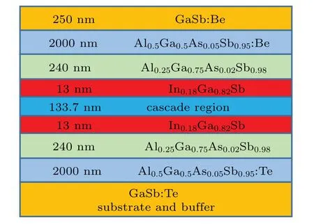
Fig.1.Full structure of type-I QW cascade laser.
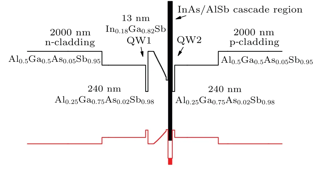
Fig.2.Band structure of the full structure.
The band structure of the cascade laser in this work is shown in Fig.2.The cladding layer and waveguide layer are similar to those of the conventional high-power quantum well lasers.[20]For conventional diode laser without cascade structure,there is only a 20-nm barrier between two quantum wells.[21]However,the cascade laser makes some differences between the two QWs.
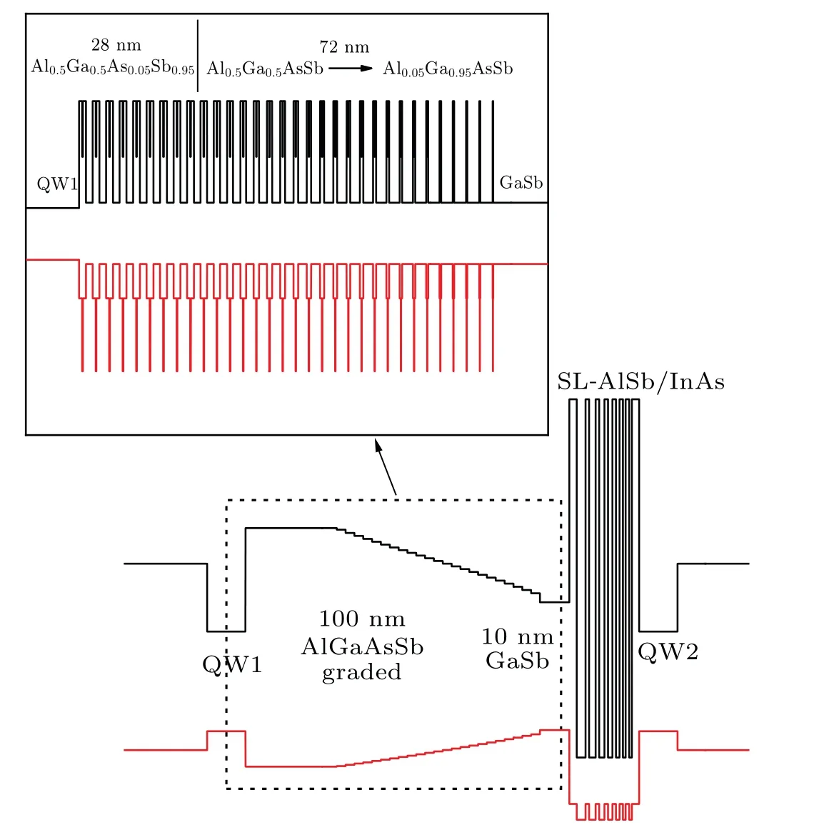
Fig.3.“Heart”of type-I QW cascade laser and gradient AlxGa1?xAsSb digital alloy.
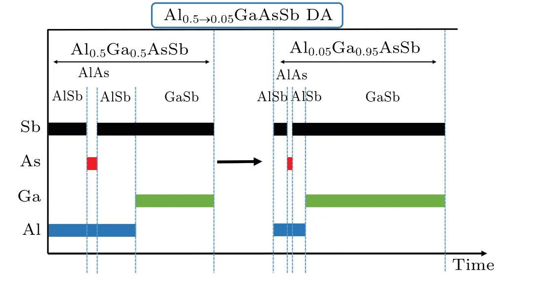
Fig.4.Shutter sequence of gradient AlxGa1?xAsSb digital alloy.
The“heart”of the type-I QW cascade laser is shown in Fig.3.The QW1 is followed by undoped AlGaAsSb with 28-nm-thick Al0.5Ga0.5As0.05Sb0.95and 72-nm-thick graded AlxGa1?xAsSb layer with x changing from 0.5 to 0.05.The AlGaAsSb graded barrier is used to prevent the electrons from transiting from QW1 to QW2 through the conduction band.The insert in Fig.3 shows the graded layer with digital alloy.One period of the digital alloys grown by short-period superlattices is about 10 monolayers(MLs)≈3.1 nm.Taking the Al0.5Ga0.5As0.05Sb0.95for example,its one period consisting of 1.44-nm-thick AlSb,1.52-nm-thick GaSb,and 0.14-nmthick AlAs is inserted in the AlSb layer to balance the lattice matching.The actual thickness of AlAs is determined by the result of high-resolution x-ray diffraction(HRXRD)to make the digital alloy of Al0.5Ga0.5As0.05Sb0.95matched with the lattice of GaSb substrate.It is identical to growing digital alloy by changing the Al composition.For the gradient AlxGa1?xAsSb,using 10 atomic layers as a cycle,the composition is controlled by adjusting the thickness of AlSb,AlAs,and GaSb,separately.[22,23]The shutter sequence of gradient layer with digital alloys is shown in Fig.4.For better understanding,the growth times of different composition short period superlattices with different Al compositions of AlxGa1?xAsySb1?ydigital alloys are shown in Table 1.The growth rates of the group-III elements used here are all 0.5 ML/s.Growing digital alloy gradient layer with short period superlattice is much simpler than directly changing the temperature of the group-III sources to grow random alloy,and growing the random alloys requires the simultaneous controlling of group-V elements to adjust strain which is a little complex.However,the digital alloy only needs to control the shutter to determine the composition.To some extent,it reduces the instability of changing the source temperature and the uncertainty of strain control.
The tunnel junction and the electron injector are followed which connected QW1 and QW2 in series rather than in parallel as shown in Fig.3.The electrons in the valence band will pass through the GaSb/AlSb/InAs tunnel junction(also called semimetallic interface in ICL)to realize the tunneling from the valence band to the conduction band and the electrons will be injected into the QW2 through the miniband of InAs/AlSb SL electron injector.The tunnel junction consists of 10-nm-thick GaSb,2.5-nm-thick AlSb,3-nm-thick InAs,and 1.2-nm-thick AlSb.And the electron injector is comprised of Si-doped(5×1017cm?3)6-period InAs/AlSb chirped SLs.The layer structure of SLs is as follows:2.2 nm-thick InAs/1.2-nm-thick AlSb/1.8-nm-thick InAs/1.2-nm-thick AlSb/1.5-nm-thick InAs/1.2-nm-thick AlSb/1.2-nm-thick InAs/1.2-nm-thick AlSb/0.9-nm-thick InAs/1.2-nmthick AlSb/0.9-nm-thick InAs/2.5-nm-thick AlSb.Then the second quantum well(QW2)of 13-nm-thick In0.18Ga0.82Sb is grown.
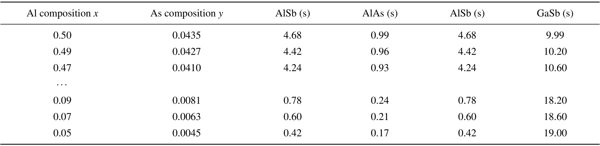
Table 1.Growth times of AlSb/AlAs/AlSb/GaSb short-period superlattices with different compositions of AlxGa1?xAsySb1?y digital alloys.
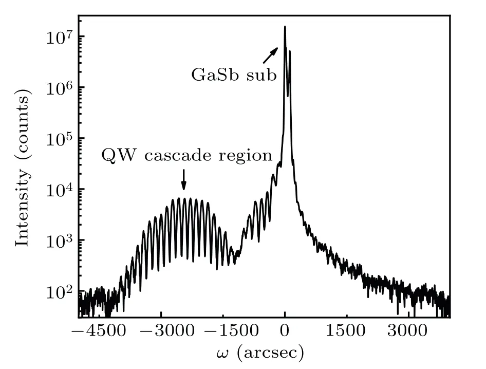
Fig.5.HRXRD spectrum of type-I QW cascade laser with QW cascade region marked.
Figure 5 shows the HRXRD curve of the quantum well cascade laser.The central peak for the Al0.5Ga0.5As0.05Sb0.95cladding layer and the Al0.25Ga0.75As0.02Sb0.98waveguide layer coincide with the substrate peak,indicating that the lattice of material matches with that of the substrate,and the clear satellite peak of QW cascade region indicates the high growth quality of the material.
3.Laser performance
By lithographing and inductively coupled plasma etching(ICP),the 2-mm-long 100-μm-wide strip ridges are fabricated.And 250-nm-thick Si3N4films are deposited for insulation by the plasma-enhanced chemical vapor deposition(PECVD).Then the p-contact electrode Ti/Pt/Au is formed by sputtering.With the substrate thinned by chemical mechanical polishing(CMP)technique,the n-contact is achieved by sputtering Au-GeNi/Au and rapid thermal process(RTP).After cleaving into 2-mm-long chips,Al2O3anti-reflection(AR<5%)and highreflection 2-pairs Si/SiO2(HR>95%)are coated.The devices were all epi-side down,and the light–current–voltage characteristics for 100-μm-wide,2-mm-long coated QW cascade laser in continuous wave at different temperatures are shown in Fig.6.
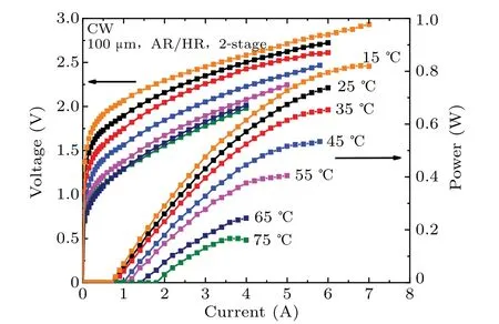
Fig.6.The L–I–V for 100-μm-wide,2-mm-long coated lasers in continuous wave at different temperatures.
Fig.7.Spectrum of room-temperature quantum-well cascade continuouswave laser at 2 A.
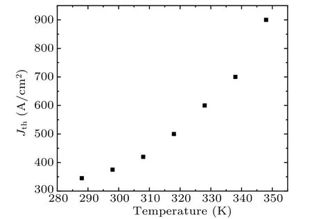
Fig.8.Variations of threshold current densities with temperatures.
The threshold current density of Jth=345 A/cm2and the maximum output power 800 mW at 15°C are achieved.The slope efficiency is estimated at 200 mW/A.The internal efficiency of the 100-μm wide two-stage cascade laser is~105%at room temperature which confirms the recycling process of carriers.The direct electron tunneling from QW1 to QW2 can be reduced by increasing the Al composition of the AlGaAsSb gradient layer and doping with Be.And by adjusting the energy levels in InAs/AlSb injector,the internal quantum efficiency can be improved.The emission spectra are measured by a Fourier-transform infrared(FTIR)method and figure 7 shows the laser spectrum of laser at 2 A at room temperature whose wavelength is near 1950 nm.Temperature dependence of Jthin CW coated laser is shown in Fig.8.Through calculation,the characteristic temperature T0≈62 K.
4.Conclusions and perspectives
In this work,we report the AlGaAsSb quaternary digital alloy with the short period superlattices,fabricated by molecular beam epitaxy.The GaSb-based quantum well cascade laser is emitted at about 2μm,and reaches nearly 800-mW output power.The characteristic temperature is T0≈62 K.We believe that the cascade structure will become more effective and have better device performance,by increasing the Al composition of gradient AlGaAsSb and changing the band structure of InAs/AlSb electron injector to change energy.
猜你喜歡
作文小學(xué)中年級(2024年2期)2024-03-02 02:23:14
電池(2022年6期)2022-02-09 09:10:53
科學(xué)與財(cái)富(2021年33期)2021-05-10 14:54:29
快樂作文(1.2年級)(2020年5期)2020-09-10 07:22:44
Journal of Donghua University(English Edition)(2020年2期)2020-06-04 06:24:12
大眾文藝(2020年7期)2020-04-21 07:03:44
作文大王·低年級(2019年10期)2019-11-25 02:34:06
金橋(2018年4期)2018-09-26 02:24:56
黨的生活(黑龍江)(2018年2期)2018-03-10 07:47:15
試題與研究·高考理綜物理(2016年3期)2017-03-28 21:08:11
- Chinese Physics B的其它文章
- Origin of anomalous enhancement of the absorption coefficient in a PN junction?
- Protection of isolated and active regions in AlGaN/GaN HEMTs using selective laser annealing?
- First-principles study of plasmons in doped graphene nanostructures?
- Probing thermal properties of vanadium dioxide thin films by time-domain thermoreflectance without metal film?
- An improved model of damage depth of shock-melted metal in microspall under triangular wave loading?
- Signal-to-noise ratio of Raman signal measured by multichannel detectors?