
Monolithic epitaxy and optoelectronic properties of single-crystalline γ-In2Se3 thin films on mica*
2021-01-21 02:08:34XiboYin尹錫波YifanShen沈逸凡ChaofanXu徐超凡JingHe賀靖JunyeLi李俊燁HainingJi姬海寧JianweiWang王建偉HandongLi李含冬XiaohongZhu朱小紅XiaobinNiu牛曉濱andZhimingWang王志明
Chinese Physics B 2021年1期
Xibo Yin(尹錫波), Yifan Shen(沈逸凡), Chaofan Xu(徐超凡), Jing He(賀靖), Junye Li(李俊燁), Haining Ji(姬海寧),Jianwei Wang(王建偉), Handong Li(李含冬),?, Xiaohong Zhu(朱小紅),Xiaobin Niu(牛曉濱),?, and Zhiming Wang(王志明)
1School of Materials and Energy,University of Electronic Science and Technology of China,Chengdu 611731,China
2College of Materials Science and Engineering,Sichuan University,Chengdu 610064,China
3Institute of Fundamental and Frontier Sciences,University of Electronic Science and Technology of China,Chengdu 610054,China
Keywords: γ-In2Se3,molecular beam epitaxy,optoelectronic response
1. Introduction
In2Se3can be considered as one of the complex III–VI compounds due to its existence in several allotropic phases, such as α-In2Se3with layered phase,[1]β-In2Se3with rhombohedral phase,[2]γ-In2Se3with defect-wurtzite structure,[3,4]and κ-phase with anisotropic structure.[5]One can find advanced applications of In2Se3of different crystal structures in diverse fields, such as phase-change storage,[6]photovoltaics,[7]optoelectronics,[8]ionic battery,[9]thermoelectrics,[10]and ferroelectronics.[11,12]Among the well-known phases of In2Se3, the defect-wurtzite γ-In2Se3exhibits large optical rotary power with a wide band gap(~2 eV), so that it holds great promise for developing novel photonic and optoelectronic devices operated at high temperature.[13,14]For device application purpose, the thin film plays a vital role;thus,there have been many methods employed to obtain γ-In2Se3thin films. γ-In2Se3thin films prepared by magnetron sputtering,source co-evaporation,chemical bath deposition, solid-phase reaction, electrodeposition,and sol-gel technologies are polycrystalline (PC) with inferior electronic and optical quality.[15–17]So far, the singlecrystalline (SC) γ-In2Se3films are only obtained by metalorganic chemical vapor deposition (MOCVD) or molecular beam epitaxy(MBE)method. However,the MOCVD growth of γ-In2Se3has to be operated at a temperature higher than 700 K,[18,19]which is incompatible with the microelectronic process required for integrating γ-In2Se3on patterned circuits.As to the MBE approach,Ohtsuka et al. obtained SC γ-In2Se3at the growth temperature higher than 573 K and the VI/III ratio between 5 and 15,using GaAs(111)B as substrate.[20]The γ-In2Se3films were proposed to be grown by the so-called van der Waals epitaxy,[20]but their crystallinity was very poor.
Despite all these efforts,the challenge remains to achieve pure phase γ-In2Se3thin films of decent material quality,due to the low phase transition (PT) barriers between In2Se3allotropies. In this study, we manage to integrate SC γ-In2Se3on mica by MBE,as an approach to achieve monolithic SC γ-In2Se3thin films at more accessible growth temperature with decent material quality. It is observed that the initial condensation of In2Se3thin layer undergoes a rapid self-organization process through which an ultrathin β-In2Se3layer is formed on mica surface at low growth temperature (450 K–500 K).The obtained ultrathin layered β-In2Se3then serves as an effective buffer layer and facilitates the subsequent phase-pinned epitaxial growth of γ-In2Se3at conditions far from thermodynamic equilibrium. The as-grown metastable γ-In2Se3thin films exhibit excellent structural stability,crystallinity,and optoelectronic properties,thus are promising for optoelectronics and photonics applications.
2. Experimental procedures
The growth of In2Se3thin films was carried out in a customized MBE chamber with a base pressure of ~3×10⁻¹⁰mbar. Fluorophlogopite mica chips with 500 μm thick Mo film coated on the back side were used as substrates. A pair of thermocouples were mounted near the sample for monitoring the growth temperature. High purity In(99.9999%)was evaporated from a standard Knudsen cell and Se(99.999%)from a crack cell,respectively.The beam equivalent pressure(BEP)of In and Se was measured by a beam flux monitor(BFM),and In flux was further calibrated by a quartz oscillation crystal (QCO) for precise surface coverage analysis. During the deposition,the Se/In beam equivalent pressure ratio was fixed at 20:1 to create a Se-rich environment.[21,23]At In BEP of ~1×10⁻⁷mbar,which corresponds to a QCO rate of ~2 monolayers (MLs)In on γ-In2Se3(0 0 1)surface per minute, a growth rate of ~1 nm (approximately a half unit cell length in c-axis of γ-In2Se3)per minute of γ-In2Se3film was achieved as further evidenced by ex situ thickness inspection by a profilometer. Noting that one unit cell of γ-In2Se3consists of 4 MLs In along c-axis,we thereby deduced thorough surface incorporation of In adatoms during epitaxial growth of γ-In2Se3.
The surface structure evolution of In2Se3during deposition was in situ monitored by reflection high energy electron diffraction (RHEED, model RHD-30, SPCES GmbH).The techniques employed to evaluate the quality of obtained γ-In2Se3films include: high-resolution x-ray diffraction(HRXRD,model Bede D1,Jordan Valley),scanning electron microscope (SEM, model InspectF, FEI), energy dispersive x-ray spectrometer (EDS, model INCA, OXFORD),atomic force microscopy(AFM,Veeco),Raman spectroscopy,and photoluminescence spectroscopy (PL, model inVia Raman Microscope, Renishaw). The optoelectronic response of the film was measured under the illumination of a class AAA solar simulator. All measurements were carried out at room temperature.
3. Results and discussion


Fig. 1. RHEED patterns taken during the growth of an In2Se3 film. The patterns are observed in the[0 1 0]azimuth of mica substrate; (a)the mica substrate,(b)the nucleation of β-In2Se3 buffer layer at In nominal coverage of ~2 MLs,and(c)γ-In2Se3 film achieved after β →γ process. (d)Ballstick illustrations of defect-wurtzite crystal structure and top In–Se bilayer structure of γ-In2Se3. The hexagonal Se- and honeycombed In-sublattices in the close-packed plane of γ-In2Se3 are indicated by solid and dotted lines,respectively.


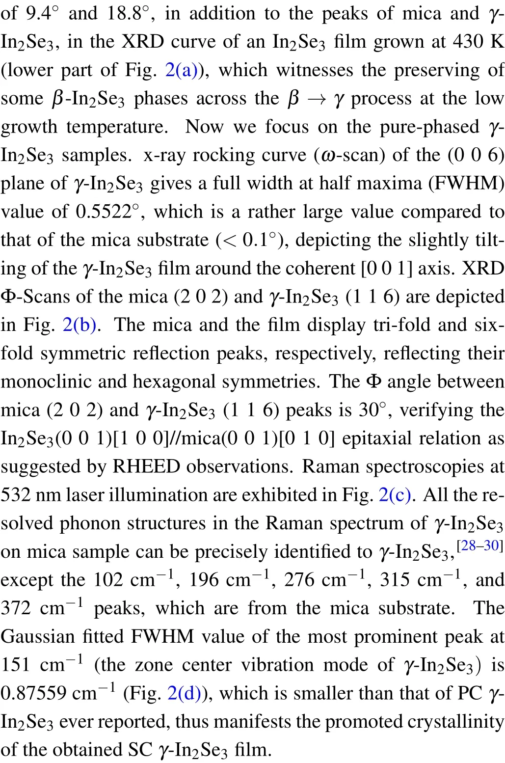


Fig.3. (a)Large-size SEM image of a γ-In2Se3 thin film deposited at the substrate temperature of 480 K and with a thickness of 60 nm.(b)A zoom-in SEM image exhibiting the stacked nanoflakes surface morphologies of the same sample. (c)EDS spectrum of the γ-In2Se3 film on mica. (d)An AFM image from the same γ-In2Se3 sample in(a).
Figures 3(a)and 3(b)display large-size and zoom-in SEM images of γ-In2Se3thin film, respectively, exhibiting deposition of microflakes of micrometer dimension and smooth surfaces stacked on one another. The AFM measurements of the same sample further reveal the surfaces of microflakes displayed in Figs. 3(a) and 3(b) are slightly rough (RMS roughness ~3 nm) and decorated with small nanocrystals(Fig. 3(d)). Such surface morphologies may reflect an outof-plane mosaic structure of the epifilm since there is lattice tilting in[0 0 1]epitaxial orientation as revealed by XRD.EDS composition study of the as-grown γ-In2Se3thin film is shown in Fig.3(c),which demonstrates the presence of In and Se.
Figure 4(a) presents the 532 nm laser-illuminated PL spectrum of the γ-In2Se3film with PL peak positioned at 1.94 eV, which is in good agreement with the previous literature.[31–33]The existence of PL spectrum depicts the production of photo-induced charge carriers, which is a vital property of semiconductor material for its application in optoelectronic/photovoltaic devices. As a proof-of-concept, a simple device is fabricated by manually pasting two In-Ga eutectic alloy electrodes to the two sides of the short edges of a 200 nm thick γ-In2Se3epifilm (with plane geometry of 10 mm×4.5 mm), respectively, to inspect the optoelectronic response under the illumination from a standard sun solar simulator (AM 1.5 G, 100 mW/cm2). The calculated resistivity from the dark I–V curve of the SC γ-In2Se3epifilm is~6×10⁴Ω·cm, which is almost 3 to 4 orders of magnitude smaller than that of PC γ-In2Se3films,[34,35]on the other hand,implying enhanced carrier mobility and/or increased carrier density of the SC film. Under the illumination of light, the current in the 200 nm thick SC γ-In2Se3film shows nearly ten times higher value compared to its value in the dark,suggesting improved photoresponse as compared to that of PC γ-In2Se3nanocrystals achieved by chemical routes.[36]Anyway, we also note that a much higher current ratio of ~50 under light and dark conditions is reported in sputtered thick PC γ-In2Se3film.[37]Because there’s commonly higher defect density in PC materials than in their SC counterparts,one cannot simply ascribe the degraded photoresponse in SC γ-In2Se3films compared with its PC counterparts to carriers trapping effects brought about by bulk defects. We thus speculate the photogenerated carrier kinetics in our SC γ-In2Se3thin films would be subjected to some surface trapping processes since the film thicknesses of the samples in our experiments are thin enough (i.e., no more than two hundred nanometers) to give a large surface area-to-volume ratio. In another experiment carried out on a thinner SC γ-In2Se3film (100 nm), we observe little photoresponse under the same illumination condition applied to the thicker sample, which in a way verifies surface states’ contribution to the photoelectric transport increases rapidly as thickness decreases. Therefore,prior to optoelectronic device applications,it should be necessary to use thick films and/or effectively passivate the surface states of SC γ-In2Se3. On the other side, the surface-sensitive optoelectronic characteristics might be favorable in photocatalytic applications of thin SC γ-In2Se3films.[38]

Fig. 4. (a) PL spectra of a 200 nm thick γ-In2Se3 thin film. (b) Currentvoltage (I–V) characteristics of the same film in the presence and absence of light(inset shows a schematic diagram of the device configuration for the measurements).
4. Conclusi ons
In summary, single-crystalline γ-In2Se3thin films are epitaxially grown on mica by molecular beam epitaxy at low temperature. An ultrathin β-In2Se3van der Waals type buffer layer is confirmed to form through a self-organization growth during initial deposition, which facilitates subsequent monolithic epitaxy of metastable γ-In2Se3. The achieved single-crystalline γ-In2Se3thin films exhibit strong roomtemperature photoluminescence and moderate optoelectronic response, thus are suitable for further device development.The method presented in this paper would lay the foundation for future epitaxial integration of γ-In2Se3on various van der Waals type materials or microelectronic circuits at deviceprocess compatible growth temperature conditions.
Acknowledgement
We thank Dr. Jing Ni and Mr. Dechao Xu for their help in preparing mica substrates.

- Chinese Physics B的其它文章
- Numerical simulation on ionic wind in circular channels*
- Interaction properties of solitons for a couple of nonlinear evolution equations
- Enhancement of multiatom non-classical correlations and quantum state transfer in atom–cavity–fiber system*
- Protein–protein docking with interface residue restraints*
- Effect of interaction between loop bases and ions on stability of G-quadruplex DNA*
- Retrieval of multiple scattering contrast from x-ray analyzer-based imaging*