
Low-tem perature grow th of large-scale,single-crystallinegrapheneon Ir(111)*
2019-05-11 07:29:58HuiGuo郭輝HuiChen陳輝YandeQue闕炎德QiZheng鄭琦
Chinese Physics B 2019年5期
HuiGuo(郭輝),HuiChen(陳輝),Yande Que(闕炎德),QiZheng(鄭琦),
Yu-Yang Zhang(張余洋)1,2,Li-Hong Bao(鮑麗宏)1,LiHuang(黃立)1,Ye-LiangWang(王業(yè)亮)1,
Shi-Xuan Du(杜世萱)1,2,?,and Hong-Jun Gao(高鴻鈞)1,2
1Institute ofPhysicsand University ofChinese Academy ofSciences,Beijing 100190,China
2CASCenterforExcellence in TopologicalQuantum Computation,University ofChinese Academy ofSciences,Beijing 100190,China
(Received 27 February 2019;revisedmanuscript received 21March 2019;published online19 April2019)
Keywords:graphene,low-temperature grow th,single-crystalline,Ir(111)
1.Introduction
Graphene,a two-dimensional atom ic crystal with a honeycomb structure,has aroused tremendous interest in both scientif ic and industrial f ields due to its extraordinary electronic,[1]mechanical,[2]and optical[3]properties.One of thew idely usedmethods to synthesize graphene is the epitaxialgrow th of graphene on transitionmetal substrates,such as Ni,[4]Ru,[5–10]Cu,[11–14]Pt,[15,16]and Ir.[17–19]Among these substrates,Ir has a comparatively low carbon solubility,[20]which is important for self-limiting grow th of graphene by thermal decomposition of hydrocarbons.[18]However,the weak interaction between grapheneand Irusually leads to the formation of polycrystalline graphene,whichmeans that there aremany domainswith different latticeorientations.[21,22]The grow thmechanism and controllable fabrication of large-scale,single-crystalline graphene on Ir(111)attracted considerable research interest.[18,23–25]
To date,thereare twomain strategies to synthesizesinglecrystalline graphene on Ir(111).The f irststrategy is to elevate the grow th temperature.[24]When the temperature exceeds 1500 K,the grow th ofm isaligned domains is suppressed and graphene with a single aligned domain is obtained.Another synthesis strategy is through an alternating exposure of ethylene and oxygen,which yields a nearly pure aligned domain of graphene.[25]However,the grow th temperature of 1126 K isstill relatively high.Asa low-temperaturegrow th technique is more econom ical,environment-friendly,and feasible for applications,the fabrication of large-scale,single-crystalline graphene on Ir(111)ata relatively low temperature is highly desirablebutchallenging.
In this work,large-scale,single-crystalline graphene is successfully fabricated on Ir(111)at a low temperature of 800 K using a three-steps fabrication route.Polycrystalline graphenewhich containsdomainsaligned/misalignedwith the Ir lattice is f irstly grown on Ir(111)surface at800 K.Then a post-treatment of exposing polycrystalline graphene to oxygen etches themisaligned graphene domains away.By using the remaining aligned domains as nucleation centers,largescale and single-crystalline graphene is f inally achieved after an additional grow th cycle at 800 K.During such grow th process,the post-treatment of exposing the polycrystalline graphene to oxygen plays a signif icant role.The high quality and single lattice orientation of the as-prepared graphene are conf irmed by low-energy electron diffraction(LEED),scanning tunnelingm icroscopy(STM),and Raman spectroscopy.Besides,we transfer the single-crystalline graphene onto SiO2substrate and fabricate back-gate f ield-effect transistors(FETs).The extracted carriermobility for electron is about 3300 cm2·V-1·s-1at room temperature.Thisoxygen-etching assisted epitaxialgrow thmethod provides away for the lowtemperaturesynthesisof large-scale,high-quality grapheneon weak-coupledmetalsubstrates.
2.M ethods
The low-temperature grow th of large-scale,singlecrystalline graphene on Ir(111)was carried out in a homebuiltultra-high vacuum-molecularbeam epitaxy(UHV-MBE)system with a base pressure lower than 2×10⁻⁹mbar.An Ir(111)substrate was cleaned by repeated cycles of sputtering and annealing until it yielded a clean surface checked by STM images.Thesynthesisprocesscontainsthreesteps.First,Ir(111)was exposed to ethylene for 100 swith a pressure of 1×10⁻⁶mbar at 800 K.Then,oxygen with a pressure of 1×10⁻⁶mbarwasvented for100 sat800K.Finally,thesamplewasexposed to ethylene foranother100 swith a pressure of 5×10⁻⁷mbar at 800 K.At each step,the sample cooled down from the annealing temperature to room temperature at a slow rateof~60 K/min.
LEED was employed with a 4-grid detector(Om icron Spectra LEED)in the UHV chamber.STM was carried outat about4 K.Raman spectroscopy was performed using a commercial confocal Ramanmicroscope(WiTec)with an excitationwavelength of532 nm.Thegraphenewas transferred by a standard electrochem ical hydrogen bubblingmethod.[26]The back-gate FETswere fabricated by an electron-beam lithography technique followed by e-beam evaporation of Cr/Au(5 nm/60 nm)as the contactelectrodes.A llelectricalmeasurementswerecarried outin avacuum chamberwith thepressure lower than 10-5mbarusing a Keithley 4200-SCSsystem.
3.Resultsand discussion
Figures 1(a)–1(c)show a schematic to illustrate the fabrication process of large-scale,single-crystalline graphene on Ir(111).Figure 1(a)shows the f irstgrow th cycle of graphene.A polycrystalline graphene f ilm is epitaxially grown on an Ir substrate by exposing ethylene at 800 K.Subsequently,the sample isexposed to oxygen atapressureof1×10-6mbarat 800 K,which preferentially etches them isaligned graphene domains,as shown in Fig.1(b). Finally,we perform an additional graphene grow th cycle(5×10⁻⁷mbar ethylene,800 K)and obtain a single-crystalline graphenemonolayeron Ir(Fig.1(c)).
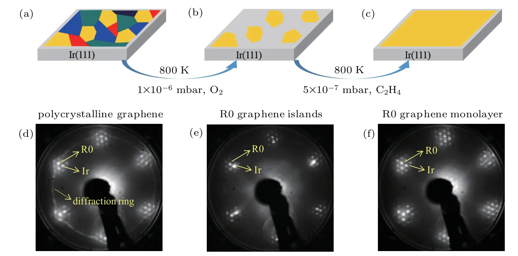
Fig.1.Fabrication process of large-scale,single-crystalline graphene on Ir(111).(a)Epitaxial polycrystalline graphene on Ir(111).(b)Remaining R0 graphene islandsafterpost-treatmentin an oxygen atmosphere.(c)R0 graphenemonolayeron Ir(111)afteradditionalgraphene grow th cycle.(d)–(f)LEED patterns(68 eV)of the sample at(a)–(c)stages,respectively.Diffraction spots contributed from R0 graphene,Ir,andmisaligned graphene(diffraction ring)are labeled.
To check the results of each step,we performed LEED measurements for thesampleatroom temperature.Figure1(d)isan LEED pattern for the sample after the f irstgrow th cycle of graphene.Two setsof diffraction spotswith the same orientation and comparable intensity(labeled by solid arrows)are contributed from aligned graphene domains(R0)and the Ir substrate.Besides,it is clear that there is a remarkable diffraction ring contributed from themisaligned graphene domains.These results reveal that the as-fabricated graphene is polycrystalline.After a post-treatment of exposing oxygen,we f ind some signif icant changes in the LEED pattern(Fig.1(e)).The diffraction ring disappears,indicating that the m isaligned graphene domains are totally etched.Moreover,the relative intensity of the spots from R0 graphene weakens,which suggests that the aligned graphene is composed of isolated islands.The results show that the oxygen preferentially etches the misaligned rather than the aligned graphene domains.One possible reason is that the interaction between m isaligned graphene and Ir isweaker than that between aligned graphene and Ir.[25,27]The LEED pattern after another grow th cycle(Fig.1(f))shows the intense diffraction spots from aligned graphene with the absence of spots from m isaligned graphene,suggesting the formation ofsinglecrystalline graphene on Ir(111).
We also carried out STM measurements to characterize the as-fabricated graphene.Figure 2(a)is a large-scale STM imageof theas-fabricated grapheneafter the f irstgrow th step.It is clear that there are two distinct graphene domains.One superstructure with a large periodicity of about 2.51 nm is aligned with the direction of Ir[1-10],which is from the R0 graphene(Fig.2(b)).The other one has a small periodicity of about0.75 nm and rotates19°relative to the orientation of Ir[1-10]labeled asR19(Fig.2(b)).These resultsconf irm that the fabricated grapheneat800K ispolycrystalline.
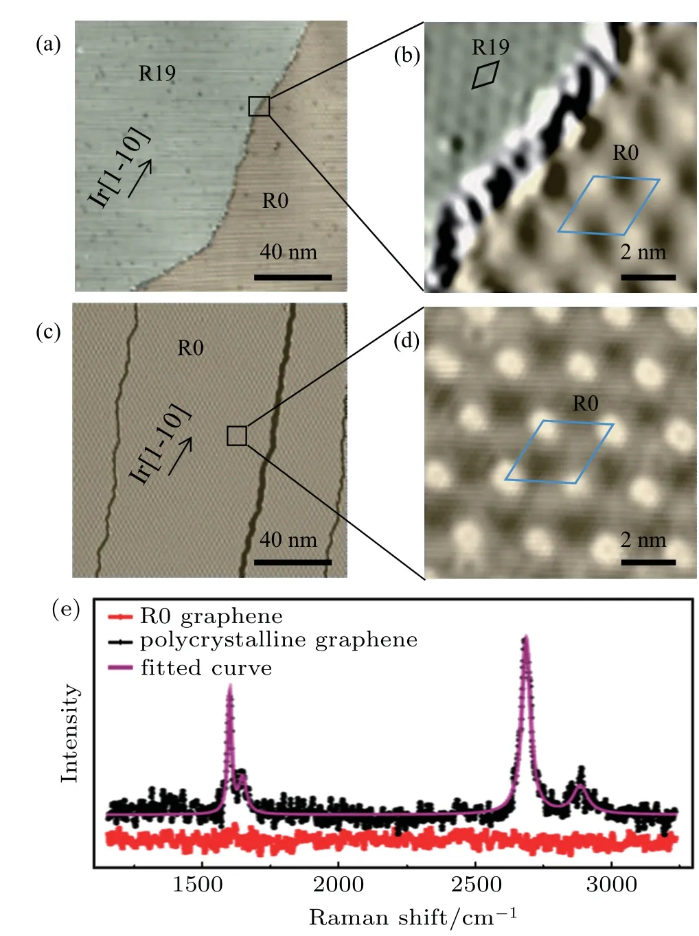
Fig.2.STM and Raman characterizations for the polycrystalline and single-crystalline graphene.(a)A large-scale STM image of polycrystallinegraphene(U=-0.2V and I=0.1 nA).(b)A zoom-in STM image shows themoir′e patternsand the domain boundary of R0 and R19 graphene(U=-0.05V and I=0.3 nA).(c)A large-scale STM image of the single-crystalline R0 graphene(U=-0.2 V and I=0.1 nA).(d)A zoom-in STM image(U=-0.05 V and I=0.3 nA).(e)Raman spectra for the polycrystalline(black dots)and single-crystalline(red dots)graphene.
TheSTM imagesof thesampleafter theextraetching(the second step)and grow th(the third step)processare shown in Figs.2(c)and 2(d).It is clear that only R0 graphene is observed.The dark lines in Fig.2(c)are steps of the Ir(111)substrate.Figure 2(d)shows a 2.51 nm moir′e pattern conf irm ing that it is R0 graphene.By checking the STM images atdifferentareas,we conf irm the formation of single-domain grapheneon Ir(111).
Raman spectroscopy isanotherpowerful tool to check the quality of graphene.It is known thatm isaligned graphene on Ir shows sim ilar Raman spectra feature as that of freestanding graphene because of the weak interaction between themisaligned grapheneand Ir substrate.[27]However,forR0 graphene on Ir,the strong hybridization betweenπelectrons of graphene and d electrons of Ir makes the Raman spectra featureless.[27]Black dots and the f itted purple curve in Fig.2(e)are the Raman spectra for the graphene after the f irst grow th step.Therearestrong G and 2D peaksconf irming that thegraphene ispolycrystalline.
Afterwe etched them isaligned graphene away and performed another graphene grow th cycle,the Raman spectrum(red dots in Fig.2(e))became featureless,indicating a singlecrystallinegraphene.Therefore,combining LEED,STM,and Raman characterizations,we conclude that we successfully fabricate the single-crystalline graphene on Ir(111)ata temperatureas low as800 K.
A detailed LEED analysis is performed to check the size of the as-fabricated single-crystalline graphene.The size of the Ir crystalused in the experiment is4mm square.The diameter of the electron beam spotof LEED is~1mm.Thus,we performed continuous LEED detection across the whole sample surface.A photo of the Ir crystal isshown in Fig.3(a).One of the four LEED patterns taken at the red circles positions1–4 isshown in Fig.3(b).
It is found that the intense diffraction spots in the four continuous LEED patterns are only contributed from R0 graphene and the corresponding moir′e pattern.There is no extra information from them isaligned graphene.To quantitative conf irm there is no extra diffraction pattern contributed from polycrystalline graphene,we also plot intensity prof iles along the arcs,which ref lect the emergence of rotational domains of LEED patterns.As shown in Fig.3(c),the upper four red prof ilesareobtained from the LEED patterns taken at the positions1–4,respectively.It isclear that there isno extra peak except the peaks related to the diffraction spots from R0 graphene in each prof ile.Asa comparison,the intensity prof ile(bottom black curve in Fig.3(c))obtained from the LEED pattern of the polycrystalline graphene shows signif icant feature contributed from m isaligned domains.These results conf irm that thewhole Ir surface is covered by single-crystalline graphene.
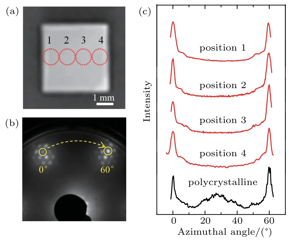
Fig.3. Continuous LEED patterns revealing a single-crystalline graphene on Ir.(a)A photo of the samplewith a size of 4mm square.Red circles represent positionswhere four continuous LEED patterns were taken.(b)Oneof the LEED patterns(68 eV)taken atpositions in(a).(c)Corresponding LEED intensity prof ilesalong thearc(from 0°to 60°).Four red prof ilesareobtained from the individual LEED patterns taken at the four positions1–4,respectively.The bottom black prof ile is obtained from the LEED pattern of the polycrystalline graphene for comparison.
Comparing to the previous study[25]which obtained nearly puresingle-oriented grapheneon Irby cyclic repetition of grow th–etching–grow th procedure using chemical vapor deposition(CVD),we achieved single-crystalline graphene through one grow th–etching–grow th cycle using UHV-MBE.There isnotonly agrow th-temperature decrease(from 1126K to 800 K)butalso a reduction of the grow th time(from about 8000 s to 300 s).The achievements of the low-temperature,fast grow th of graphene single-crystal on Ir are attributed to the ultraclean environment of UHV-MBE and the treatment of low ethylene pressure in the second grow th process.The aligned graphene nuclei(remained aligned graphene islands after oxygen-etching step),ultraclean grow th environment as well as lowered ethylene pressure play crucial roles in preventing theappearanceof them isaligned graphene in the third step.
For application purpose,we also transfer the as-grown large-scale,single-crystallinegraphene to a SiO2/Sisubstrate.Figure 4(a)is an optical image of the transferred graphene.The graphene keepshigh quality exceptsome contam inations introduced in the transfer process(bright spots in Fig.4(a)).The Raman spectrum of the transferred graphene(Fig.4(b))showssharp G and 2D bands.The intensity ratio of2D band to G band(I2D/IG)isabout4.7,indicating that thegraphene isa monolayer.[28]The intensity ratioofD band toG band(ID/IG),which ref lects the defect number of graphene,is shown in Fig.4(c).An averagevalueof0.33 revealsa low defectdensity of the transferred graphene.In addition,we f ind that the hydrogen bubbling transfer process does notdestroy the Ir(111)crystal.The Ir(111)substrate can be repeatedly used to fabricatehigh-quality single-crystallinegrapheneby the oxygenetching assisted grow thmethod.
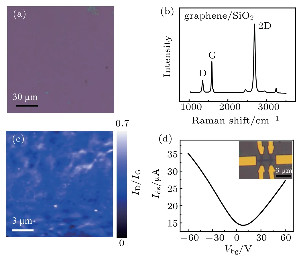
Fig.4.Single-crystalline graphene transferred onto a SiO2 substrate.(a)An optical image of the transferred graphene,show ing the continuous graphene f ilm with a few contam inations.(b)Raman spectrum of the transferred graphene on SiO2.The fullw idth at halfmaximum is smaller than 30 cm-1.(c)Ramanmapping(15μm×15μm)for the intensity ratio of D band to G band(I D/I G).(d)Source–drain current I ds versus back-gate voltage V bg at room temperature.The inset is the optical imageof the FET.
Using the transferred graphene on SiO2,we fabricated back-gated FETs.The optical image of a device is shown in the inset of Fig.4(d).The source–drain current(Ids)as a function of back-gate voltage(Vbg)ismeasured and shown in Fig.4(d).It is found that the currentminimum is shifted toward positive Vbg,indicate that the transferred graphene is p-type doped. The extracted carrier mobility is about 3300 cm2·V-1·s-1for electron and 2500 cm2·V-1·s-1for hole,which also indicates that the graphene fabricated in this method isofhigh quality.
4.Conclusion
In summary,using the oxygen-etching assisted epitaxial grow thmethod,we fabricate single layergrapheneon Ir(111)ata low temperatureof800K.Using LEED,STM,and Raman characterizations,we conf irm that the as-fabricated graphene is large-scale,single crystalline,and high quality.Moreover,we transfer the fabricated graphene on SiO2/Siand achieve a carriermobility ofabout3300 cm2·V-1·s-1at room temperature.Thiswork isof signif icance to theeff icient fabrication of wafer-scale,single-crystalline graphene on weak-interaction transitionmetalsubstrates.
- Chinese Physics B的其它文章
- Computational study of inverse ferrite spinels
- Effectsof chem icalpressure on dilutedmagnetic sem iconductor(Ba,K)(Zn,M n)2As2*
- Particle–hole f luctuationsand possible superconductivity in dopedα-RuCl3*
- Surface stabilized cubic phaseof CsPb I3 and CsPbBr3 atroom tem perature*
- Raman scattering study ofmagnetic layered M PS3 crystals(M=M n,Fe,Ni)*
- Low tem perature Pmmm and C2/m phases in Sr2CuO3+δ high temperature superconductor*