通過晶圓片檢測MEMS器件
2010-10-24 05:08:00AxelEschenburgTaufiqHabib
電子工業(yè)專用設(shè)備 2010年2期
Axel Eschenburg,Taufiq Habib
(Viscom AG,Germany)
In semiconductor manufacturing,automatic wafer inspection is essential to detect defects in the early stage.At the back-end of processes where bonding joins two or more wafers,or a wafer to a non-transparent surface,it is difficult to verify bonding results,or to inspect for contamination between the bonded surfaces.This is because silicon and other semiconductor materials are opaque to the visible and shorter wavelengths used for surface inspection.
O ne special application is MEMS inspection.MEMS comprise mechanical elements,sensors,and electrical circuits combined on a single substrate or chip.Detecting defects within the device structure is vital to ensure their operation;many of the mechanical properties cannot be verified by electrical or functional testing.As the defects are often located within the substrate or in the bond between device and cap wafer,a purely optical inspection is insufficient.Therefore,near-infrared (NIR) is a non-destructive method to detect faults on and beneath the surface.Theoretically,all defects can be detected with this technology;e.g.detection of particles (contamination),measurement of etch lines and alignment marks,structures,completeness,voids and also the quality of the frit,to name just a few (Figure 1).
1 Available Technologies

Figure 1 Silicon wafer(courtesy of IMEC.)
Various technologies are currently available for inspecting bonded MEMS wafers;each offers a different set of challenges and results.
Acoustic inspection uses an ultrasonic transducer to scan the wafer for defects that modify the reflection of sound waves.Because sound is the imaging medium,acoustic inspection excels at finding voids and cracks,while being relatively coarse with lateral resolution.This shortcoming can go so far as misrepresenting the size of defects on an ultrasonic scan.To obtain such a scan,the wafer needs to be immersed in a sound-conducting liquid,usually distilled water.This requires a cleaning step after the sonic scan is generated,while limiting application to wafers which will not be contaminated by immersion.
Long-wave infrared light can also be used to image a wafer.In this case,transmissive imaging is commonly used;silicon is transparent to long wave IR light,usually generated by halogen lamps with IR filters.Specially designed sensors are used to capture the transmitted light and generate images for analysis.Restrictive factors for this scenario are the comparatively low resolution limit as defined by Raleigh1,as well as the availability of high speed,high-resolution sensors for imaging.
A third option is X-ray inspection.Micro-or nanofocus tubes are used to generate a medium-strength X-ray radiation,which in turn is sent through the wafer and imaged with a conventional imaging chain using an image intensifier and a CCD camera,scintillator,or digital X-ray detector.Due to the short wavelength,the theoretical resolution exceeds that of both longer wavelength IR and acoustic inspection systems.Limitations for X-ray inspection stem mostly from the need to shield the entire system.Such shielding requires a lead enclosure with access limitations and enhanced security measures,which complicates sample handling.A second limitation is the high transmissivity of silicon under X-ray radiation,which results in low image contrast,making it difficult to distinguish defects from structures.
2 New Approaches
In addition to the technologies described above,there is another approach using narrow band NIR light.NIR inspection of wafers requires a solid state light source,IR-capable optics,and sensors capable of imaging with NIR light at high speeds and resolutions.Only in recent years have light sources with adequate intensity and sensors with sufficient sensitivity and resolution been developed to be used with NIR light(Figure 2).
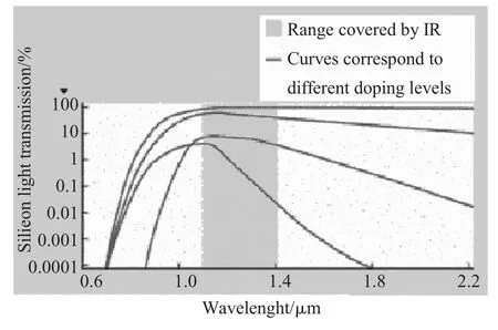
Figure 2 Optimal wavelength range for maximum transmissibility through silicon
2.1 Defect Catagories and Visual Representation
Experience has shown that NIR technology is capable of detecting several critical defects in MEMS production processes.Additionally,NIR technology allows measurement of production-related structures within the bonded wafer.The following details key elements.
2.2 Particles
Particles may occur in three positions on the wafer:on the top and bottom surfaces,or inside the wafer.The third position is particularly relevant here,since visible and UV light inspection can detect particles on the top and bottom of the wafer.NIR provides the ability to detect particles between the two bonded wafers.These particles can be distinguished from those on either surface of the bonded wafer by combining the results of NIR with darkfield visible light inspection.Since the wafer is viewed through,particles appear as dark against a brighter background.Even shards of silicon will have this effect,due to their sharply angled surfaces.Using a trained image and sophisticated algorithms,particles can be distinguished against the background of microstructures and bonding agents.
2.3 Eutectic/ Fusion Bond
In this case,two wafers are joined without introducing a foreign substance between them.Therefore,bleed-in or bleed-out is rarely an issue with this kind of bonding.Eutectic or fusion bonded wafers are also less likely to suffer from delamination,but voids are still a major cause for concern.The ability to pinpoint position,size and in some cases,even the thickness of the void allows the process to continue around the di e affected by the voids,rather than forcing processing of the entire wafer to stop.
2.4 Frit Defects
Due to frit application and also the bonding process,various types of defects are produced within the frit:
Voids,e.g.large scale areas where frit integrity is compromised by bubbles of air or foreign materials.
Delamination,where the bonding between frit and device or cap wafer is incomplete.Delamination is particularly critical as it does not initially result in a defect,but will drastically increase the risk of failure during operation.The structure of the delamination is mostly invisible to acoustic or X-ray inspection.
Bleed-in,where the frit material has bled into the active area of the die,possibly changing its mechanical or electrical characteristics.Bleed-in can usually be detected in functional tests,although borderline cases may affect device reliability.
Bleed-out,which signifies a reduction of frit width,usually in or near the corner of a die.Obviously,this reduction will increase the risk of premature failure while not necessarily showing up as a defect during acoustic or functional tests.
2.5 Frit Measurement
Various methods used for bonding wafers include eutectic,fusion,frit,etc.Frit bonding as commonly used in MEMS devices requires a material,usually a special type of glass,to be used as the fusing element between the two wafers.Glass beads can be screen-printed or sprayed onto select areas of one wafer.During the bonding process,temperature and pressure combine to melt the glass and fuse the wafers together.After the bond is complete,it is not possible to inspect bond quality using visible light(Figure 3).
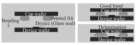
Figure 3 MEMS construction—glass frit bonding
2.6 Etch Lines
E tch lines are created in a chemical bath.This makes it unnecessary to inspect every line,but a sub sampling of selected points on the lines to verify process integrity is worthwhile.This inspection can be done with better resolution right after the etching process and before bonding,but would require the use of expensive equipment.It can,on the other hand,be included with other NIR inspection tasks.Possible qualifiers for etch lines are line width,position,distance from other lines,and distance from alignment marks.
2.7 Alignment Marks
Alignment marks are present on both the device and the cap wafer;these are checked by the bonder before the bonding process.Thus an additional check would not be required,yet misalignment may occur as an error during the bonding process.As NIR can penetrate both layers,it allows evaluation of the absolute alignment mark position of device and cap wafer,while also enabling a relative position check simply by inspecting the overlaid pattern of both marks.
2.8 Macro Structures
Depending on the actual resolution,IR inspection even allows for measurement of macroscopic structures within the active area of the die.Typically,measurement accuracy ranges from 5 to 0.7 μm.While this is inadequate to fully qualify the active area of a die,it can still serve to ensure that no macroscopic defects are present at this stage in the process.Alone,it would not warrant its own inspection stage,but as an additional benefit in a machine inspecting for the above-mentioned defects,it does bring added value to the system.
3 Conclusion
N IR is a promising new technology for quality control in the semiconductor industry.It not only has a place in the list of available technologies,but also offers new possibilities,especially in the inspection of internal structures.And this is exactly why infrared inspection is especially relevant for the non-destructive inspection of MEMS.Therefore inspection machines? that are equipped to perform this type of inspections are important to the MEMS manufacturing process(Figure 4.)
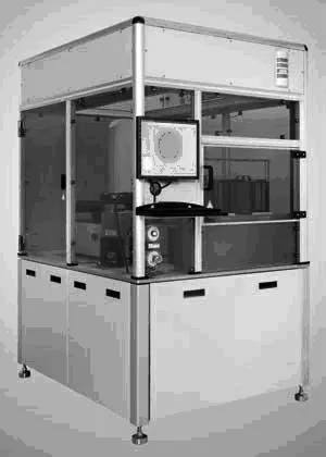
Figure 4 High precision,fully automatic wafer inspection with handling unit
1.The Raleigh criterion,named after its inventor John William Strutt,3rd Baron Rayleigh,is an empirically generated function describing the maximal resolution that can be achieved with a given optical setup.For industrial imaging described in this article,it sets the resolution R to be 0.6×the wavelength used for inspection,divided by the numerical aperture of the lens setup.
猜你喜歡
中學(xué)生數(shù)理化·七年級數(shù)學(xué)人教版(2021年6期)2021-11-22 07:50:58
中學(xué)生數(shù)理化·七年級數(shù)學(xué)人教版(2021年6期)2021-11-22 07:50:58
中學(xué)生數(shù)理化·七年級數(shù)學(xué)人教版(2021年6期)2021-11-22 07:50:58
中學(xué)生數(shù)理化·七年級數(shù)學(xué)人教版(2020年12期)2021-01-18 06:57:46
中學(xué)生數(shù)理化·七年級數(shù)學(xué)人教版(2020年12期)2021-01-18 06:57:46
光學(xué)精密工程(2016年6期)2016-11-07 09:08:13
海峽科技與產(chǎn)業(yè)(2016年3期)2016-05-17 04:32:12
焊接(2016年7期)2016-02-27 13:05:07
北京信息科技大學(xué)學(xué)報(自然科學(xué)版)(2016年6期)2016-02-27 06:31:54
電子工業(yè)專用設(shè)備(2015年4期)2015-05-26 09:10:31