
Spin transport characteristics modulated by the GeBi interlayer in Y3Fe5O12/GeBi/Pt heterostructures
2024-02-29 09:19:22MingmingLi李明明LeiZhang張磊LichuanJin金立川andHaizhongGuo郭海中
Chinese Physics B 2024年2期
關(guān)鍵詞:張磊
Mingming Li(李明明), Lei Zhang(張磊), Lichuan Jin(金立川), and Haizhong Guo(郭海中),3,?
1Key Laboratory of Materials Physics,Ministry of Education,School of Physics and Microelectronics,Zhengzhou University,Zhengzhou 450052,China
2State Key Laboratory of Electronic Thin Films&Integrated Devices,University of Electronic Science and Technology of China,Chengdu 610054,China
3Institute of Quantum Materials and Physics,Henan Academy of Sciences,Zhengzhou 450046,China
Keywords: spin current,Y3Fe5O12/GeBi/Pt heterostructures,spin pumping,inverse spin Hall effect
For the past few years, germanium-based semiconductor spintronics has attracted considerable interest because of its potential for integration into mainstream semiconductor technology.[1,2]The main challenges in the development of modern semiconductor spintronics are the generation, detection, and manipulation of spin currents.[3–10]The manipulation of a pure spin current results in low-cost energy and high-efficiency electronics.Compared with the traditional spin-injection method that introduces a spin-polarized charge current,[11–15]in a ferromagnet(FM)/nonmagnetic(NM)material structure, ferromagnetic resonance (FMR)-driven spin pumping can generate a pure spin current without a charge current via the angular momentum transfer from FM to NM material.[16–20]This dynamic coupling process is generally understood as the exchange interaction between the precessing magnetization of the ferromagnet and the conduction electrons of the normal metal at the interface region.[21,22]
Inverse spin Hall effect(ISHE)measurements are widely employed to detect the change in the spin current from the extracted dc inverse spin Hall voltage.The efficiency of spin pumping is quantified by the spin-mixing conductance parameter.[23]Modulation of spin transport in semiconductors and the fabrication of advanced spintronic devices have always been the focus of semiconductor spintronics research.Cerqueiraet al.reported the important role played by the localized states at the MgO–Si interface for the generation of spin currents in hybrid metal–silicon–metal vertical structures.[4]Kalappattilet al.reported an enhancement in the spin current through an interface organic semiconductor in a Y3Fe5O12(YIG)/C60/Pt heterostructure.The presence of C60not only decreases the conductivity mismatch between YIG and Pt, but also reduces the surface perpendicular magnetic anisotropy of YIG.[24]However,the underlying mechanism of spin-current transmission in semiconductors is not fully understood and needs further clarification.
By considering the integration of spintronic devices into traditional semiconductor mainstream technology, we have fabricated a series of Ge1-xBix(x=0.04,0.07,0.11,and 0.15)films and investigated the transport characteristics of the spin current in Y3Fe5O12/GeBi/Pt heterostructures.The extracted inverse spin Hall voltage shows an exponential decay with the increase in the semiconductor barrier thickness.Different Bi concentrations could be used to tune the band gap and the spin decay length of GeBi films.Furthermore, the spin-injection efficiency is also dependent on the band gap of the GeBi barrier.Our results will provide an efficient method to improve the spin-injection efficiency in semiconductor materials.
High-quality YIG single-crystal films were epitaxially grown on (111) Gd3Ga5O12substrates with a thickness of 200 nm by liquid phase epitaxy.The Ge1-xBixfilms were deposited using molecular beam epitaxy at a basic vacuum pressure of 4×10⁻⁹Torr.The Ge source temperature was fixed at 1200?C.The Bi source temperatures were maintained at 425?C, 450?C, 475?C, and 485?C, and the corresponding Bi concentrations were 4%, 7%, 11%, and 15%.During the growth of GeBi films,the substrate temperature was maintained at 150?C to allow Bi atom incorporation in the Ge lattices without Bi precipitation or agglomeration.Figure 1(a)shows the x-ray photoelectron spectroscopy (XPS) full spectrum of GeBi films.The main elements are found to be Ge,Bi,and C.The presence of carbon(C)is inevitable and was used for data calibration.Moreover, the element proportion of the film was determined by fitting the peak area of Bi 4f and Ge 3d.The phase formation of GeBi films with different Bi content was characterized by x-ray diffraction (XRD), as shown in Fig.1(b).There are two diffraction peaks corresponding to GeBi along the(012)direction around 27.1?and the(104)direction around 38.2?.It is well known that the atomic radius of Bi is bigger than that of Ge.When the content of Bi increased from 4%to 15%,the diffraction peak of GeBi moved towards a lower diffraction angle, which means the Bi atom was incorporated into the Ge lattice.The transmission electron microscopy(TEM)results of the interfacial region in the YIG/Ge0.85Bi0.15bilayer are shown in Fig.1(c).It is observed that the interface is atomically sharp.Figure 1(d) shows the distribution of Fe,Ge,and Bi elements at the interface region.There is no element diffusion at the interface.

Fig.1.The XPS, XRD and TEM results of GeBi (100 nm) in the YIG/GeBi bilayer.(a) The XPS full spectrum of Ge0.85Bi0.15 in the YIG/Ge0.85Bi0.15 bilayer.(b) The XRD scans of GeBi films with different Bi contents.(c) The TEM image of the interfacial region in the YIG/Ge0.85Bi0.15 bilayer.(d)The distribution of Fe,Ge,and Bi elements at the interface region.
We investigated the spin-pumping efficiency of the Y3Fe5O12/GeBi/Pt heterostructures using a wideband ferromagnetic resonance (FMR) system.The microwave power was fixed at 10 dBm to avoid the influence of nonlinear effects that may appear under high power.The microwave frequency ranged from 2 GHz to 15 GHz to ensure the reliability of our data fitting.The FMR measurements were carried out using a coplanar waveguide(CPW)at room temperature with in-plane field sweeping.The magnetization dynamics of YIG can be described by the Landau–Lifshitz–Gilbert equation[23]
whereMis the magnetization vector ofMsandnis the unit vector parallel toM.Here,γis the gyromagnetic ratio,Heffis the sum of internal and externalHfields andαis the Gilbert damping constant.In these conditions,the spin current is generated at the YIG/GeBi interface, while the precessing magnetization of YIG acts as a peristaltic spin pump.This results in dynamic spin accumulation diffusing away from the interface.Moreover, the generation of a spin current is directly reflected as damping enhancement of YIG.We measured the FMR linewidth(?H)as a function of the microwave frequency(f) of bare YIG, YIG/Pt and YIG/Ge1-xBix/Pt samples, as shown in Fig.2(a)and fitted according to[25–28]
where g,μB, andtYIGrepresent the Lande factor, the Bohr magneton, and the thickness of the YIG layer, respectively.The damping constant for bare YIG (αYIG) is 1.1×10⁻⁴.The calculated effective damping constant and effective spinmixing conductance are shown in Fig.2(b).The damping constant increases gradually to 5.6×10⁻⁴in the YIG/Ge1-xBix/Pt samples when the Bi content reaches 15% (x=0.15).The effective spin-mixing conductance also shows similar trends.The spin-injection efficiency is about three times when the Bi content increases from 4% to 15%.Low spin-injection efficiency has always been the main factor that limits the applications of semiconductor spintronic devices.The effective spinmixing conductance in YIG/Ge0.85Bi0.15/Pt is 8.3×10¹⁸m-2,which is close to that in YIG/Pt(9.2×1018m-2).We achieved efficient spin injection at the FM/semiconductor interface by tuning the doping content of Bi in the GeBi films.

Fig.2.(a)The FMR linewidth as a function of the microwave frequency of bare YIG, YIG/Pt and YIG/Ge1-xBix/Pt samples.(b) The calculated effective damping constant and effective spin-mixing conductance of YIG/Ge1-xBix/Pt samples.
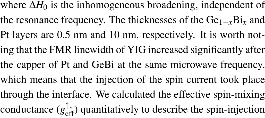
The inverse spin Hall effect directly reflects the amount of spin current injected into the Pt layer and is easy to measure.Normal metal like Pt has strong spin–orbit coupling and a large spin Hall angle (θSH), in which the pumped spin current is converted into a DC charge current by the inverse spin Hall effect.To determine the underlying mechanisms in the spin transport characteristics in the GeBi semiconductor, we measured the inverse spin Hall effect of the YIG/Ge1-xBix/Pt samples.Figure 3(a) shows a schematic of the inverse spin Hall effect measurement setup.Similar to the FMR measurements, the inverse spin Hall voltage (VISHE) was measured at room temperature with in-plane field sweeping.The rf fieldhrfis perpendicular to the coplanar waveguide signal line.Here,θHis the angle between the external magnetic fieldHand the measuredVISHE.WhenθH=90?the measured inverse spin Hall voltage can be expressed as[22,31,32]
whereeis the electron charge,andρ,wandλSDare the resistivity of the Pt layer,the spin Hall angle,the CPW signal line width and the spin diffusion length,respectively.Here,dis the thickness of the Pt layer,which is fixed at 10 nm;θis the magnetization precession cone angle,as shown in Fig.3(a);andPis the ellipticity correction factor arising from the ellipticity of the magnetization precession.The microwave frequency and power were set at 5 GHz and 10 dBm,respectively.Figure 3(b)shows the measuredVISHEaround the resonance field of the YIG/Ge0.85Bi0.15(0.5 nm)/Pt(10 nm)sample.The measured voltage curves are Lorentz symmetric, and we also reversed the magnetic field to avoid interference from thermal effects.We also studied the effects of the Bi content on the inverse spin Hall voltage, as shown in Fig.3(c).TheVISHEincreases almost linearly when the Bi content increases from 4%to 15%in GeBi films.We investigated the spin transport characteristics through the GeBi layer by changing the thickness of the GeBi barrier layer.We measured the inverse spin Hall voltage as a function of the Ge1-xBixthickness, which ranges from 0.5 nm to 4 nm,as shown in Fig.4(d),and the curves here are the fitting results using the following function(5).For a given Bi content,the inverse spin Hall voltage decays exponentially with the increase in the GeBi thickness.
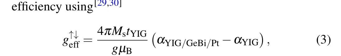
To establish the exponential decay model of the spin current in the semiconductor layer, we introduced the parameter decay length(λ).The inverse spin Hall voltage as a function of the GeBi thickness(dGeBi)is expressed as
whereVISHE(dGeBi= 0) is the inverse spin Hall voltage of the YIG/Pt sample.The fitted decay length parameters as a function of the Bi content are shown in Fig.4(a).The Bi content shows a strong modulation effect on the decay length,i.e.,the spin transmission characteristics within the semiconductor barrier.We obtained a decay length of 1.98 nm in Ge0.85Bi0.15;however,the decay length reduces to 0.80 nm in Ge0.96Bi0.04.A higher Bi content is favorable for spin transport in GeBi films.Combined with the results of the above spin-pumping measurements, we found that both the calculated spin decay length and effective spin-mixing conductance increased with the Bi content.Figure 4(b)further shows the relationship between the spin decay length and damping enhancement,which indicates that the spin transfer inside the semiconductor is also related to the spin injection through the YIG/semiconductor interface.
When we consider the characteristics of the spin-pumping mode and the YIG’s insulating properties, the spin current in the YIG/GeBi/Pt structures is expected to come from the exchange interaction between the conduction electrons of Pt and the processing magnetization of YIG.Thus, the spin transport characteristics are sensitive to the band gap of the semiconductor barrier.[33]The near-infrared properties of the YIG/Ge1-xBixsamples with different Bi content were used to identify the band gap of the doped semiconductor thin films.The absorption spectra for Ge1-xBixfilm, as shown in Fig.4(c), was transformed from the diffuse reflectance(R)spectra using the Kubelka–Munk function[33]
Fig.3.(a)A schematic of the inverse spin Hall effect measurement.(b)The VISHE around the resonance field of the YIG/Ge0.85Bi0.15(0.5 nm)/Pt(10 nm) sample.(c) The VISHE as a function of the Bi content in YIG/Ge1-xBix/Pt samples, and (d) the VISHE as a function of the Ge1-xBix barrier thickness.
Fig.4.(a)The fitted spin decay length as a function of the Bi content.(b)The relationship between the spin decay length and damping enhancement.(c)The absorption spectra of Ge1-xBix film.(d)The spin decay length as a function of the band gap in YIG/Ge1-xBix/Pt structures.
The band gap was extracted at the intersection of the linear fit and photon energy axis.The enhancement of doped Bi causes a decrease in the band-gap of Ge1-xBixfilms,which is similar to the results presented in a previous study of GeSn, another Ge-based semiconductor.[34]The band gap of Ge0.96Bi0.04is found to be 0.65 eV and subsequently reduced to 0.55 eV in Ge0.85Bi0.15films.Figure 4(d)shows the spin decay length as a function of the band gap in the YIG/Ge1-xBix/Pt structures.The smaller barrier band gap corresponds to the longer spin decay length.Furthermore,one may notice that both the characteristics of spin transfer inside the semiconductor(Fig.4(a))and the spin injection through the interface (Fig.4(b)) for Ge0.85Bi0.15have more significant changes compared to those with low Bi content (4% to 11%).This may be due to the change in the band-gap type.Ge itself is an indirect band gap semiconductor and gets converted into a direct bandgap material when the Sn doping reaches a certain doping concentration.[35]A similar transformation might have occurred in the GeBi films.
In conclusion,we manipulated the band gap of Ge1-xBixfilms by changing the doping concentration of Bi and investigated the spin transport characteristics in YIG/Ge1-xBix/Pt structures.The spin current through the semiconductor barrier showed an exponential decay with the increase in the barrier thickness.The spin-injection efficiency at the YIG/Ge1-xBixinterface increased with the Bi content.We identified the band gap of Ge1-xBixfilms and found that the band gap of the semiconductor barrier plays an important role in the spin-injection efficiency through the YIG/semiconductor interface and also the transportation within the semiconductor barrier.Our findings provide a method to improve spin-injection efficiency at the FM/semiconductor interface and offer potential guidance for the combination of mainstream semiconductor technology and spintronics.
Acknowledgments
Project supported by the National Key Research and Development Program of China(Grant No.2021YFA0718701),the China Postdoctoral Science Foundation (Grant No.2022M722888), and the National Natural Science Foundation of China(Grant Nos.12174347 and 12004340).
猜你喜歡
中國民間療法(2021年19期)2021-11-20 06:22:32
Chinese Physics B(2021年6期)2021-06-26 03:04:32
北極光(2020年1期)2020-07-24 09:04:06
Acta Mathematica Scientia(English Series)(2018年2期)2018-05-05 07:09:39
北方文學(2018年2期)2018-01-27 13:54:48
幸福(2016年6期)2016-12-01 03:07:57
車迷(2015年6期)2015-03-20 02:43:54
傳奇·傳記文學選刊(2014年8期)2014-10-30 05:04:51
中醫(yī)研究(2014年8期)2014-03-11 20:29:20
中醫(yī)研究(2014年4期)2014-03-11 20:28:38
- Chinese Physics B的其它文章
- Quantum synchronization with correlated baths
- Preparing highly entangled states of nanodiamond rotation and NV center spin
- Epidemic threshold influenced by non-pharmaceutical interventions in residential university environments
- Dynamical behavior of memristor-coupled heterogeneous discrete neural networks with synaptic crosstalk
- Dynamics and synchronization in a memristor-coupled discrete heterogeneous neuron network considering noise
- Spatial search weighting information contained in cell velocity distribution