
Improving dynamic characteristics for IGBTs by using interleaved trench gate
2023-12-15 11:51:28YiFanWu吳毅帆GaoQiangDeng鄧高強(qiáng)ChenTan譚琛ShiWeiLiang梁世維andJunWang王俊
Chinese Physics B 2023年12期
Yi-Fan Wu(吳毅帆), Gao-Qiang Deng(鄧高強(qiáng)), Chen Tan(譚琛),Shi-Wei Liang(梁世維), and Jun Wang(王俊)
College of Electrical and Information Engineering,Hunan University,Changsha 410082,China
Keywords: insulated gate bipolar transistor(IGBT),dynamic avalanche(DA), dIC/dt
1.Introduction
Insulated gate bipolar transistors(IGBTs)are widely used in medium- and high-voltage power applications, such as smart grid,industrial motor drives,automotive,etc.[1-3]In order to improve the trade-off between ON-state voltage drop(Von)and turn-off loss(Eoff),many techniques have been proposed, such as field stop IGBT (FS-IGBT),[4]injection enhanced gate transistor (IEGT),[5-7]carrier stored trench-gate bipolar transistor (CSTBT),[8-10]super junction (SJ) trench IGBT.[11,12]With the decrease of turn-off loss,IGBTs are increasingly used in high frequency applications.However,high frequency is accompanied by high dV/dt, which can induce voltage overshoot and dynamic avalanche (DA) during turnoff.[13]The trench clustered IGBT (TCIGBT) structure has been proposed to eliminate DA by using a self-biased builtin p-MOSFET to divert the hole current.[14,15]Besides, high switching frequency can also lead to high dIC/dt.[16]To suppress dIC/dtwithout sacrificing the turn-on loss, some IGBTs with unique gate geometry were proposed, such as the split-gate IGBT[17,18]and the fin p-body IGBT.[19]Furthermore,clamping the floating p-body adjacent to the trench gate also helps improve the trade-off relationship between dIC/dtandEon.[20,21]
In this work,a novel trench-gate IGBT is proposed to obtain better switching characteristics.The proposed IGBT features a split-gate architecture.The poly gate and poly emitter are alternately arranged along the trench.Some paralleled self-biased p-MOSFETs are formed on the emitter side.During turn-off operation,the p-MOSFET turns on adaptively and provides an additional path for the hole current.The maximum electric field and impact ionization rate decrease greatly, thereby improving the ability to withstand the dynamic avalanche.During turn-on operation, the potential of the p-ring region below the trench gate is clamped.This can reduce the self-charging displacement current (IGdis) of the gate capacitor and the dIC/dtas well.Moreover, the interleaved gate architecture can reach a 67% reduction in Miller capacitance and a 34%increase in input capacitance, leading the turn-off loss to decrease and dIC/dtto lower.
2.Device structure and mechanism
Figure 1(a)shows the schematic diagram of the proposed IGT IGBT.The poly gate and poly emitter are alternately arranged in the trench along thezdirection as shown in Fig.1(b).Figure 1(c)shows the built-in p-MOSFET,which is composed of the p-body, n-CS layer, p-ring region, and trench emitter.The source region of p-MOSFET is the p-ring region.The p-channel is the n-CS layer.The gate and the drain of the p-MOSFET are both grounded.Figure 1(d)shows cross-section of the IGT IGBT along the cutline along BB′.Figure 2 shows the conventional CSTBT and the p-ring IGBT.[22,23]The key parameters of three IGBT structures are listed in Table 1.The models used in simulations include Philips unified mobility model,high-field saturation model,Enormal model,Slotboom model,Shockley-Read-Hall model,Auger model,and Lackner’s avalanche generation model.1300 V whenNCSis higher than 1.0×1015cm-3.Compared with the CSTBT,both the p-ring IGBT and the IGT IGBT can increase doping concentration of the n-CS layer(NCS)without any penalty onBV.This is because the p-ring region can effectively alleviate the electric field at the bottom of the trench.However, with the increase ofNCS, the safe-operating area(SOA)of p-ring IGBT degrades.The saturation current of pring IGBT is extremely sensitive toNCSas shown in Fig.4(b).To achieve wide forward biased(FB)SOA,theNCSof p-ring IGBT should be limited below 3.5×1016cm-3.Comparing with the CSTBT, The saturation current of IGT IGBT is reduced by 27%owing to the addition of p-channel and the decrease of n-channel width.
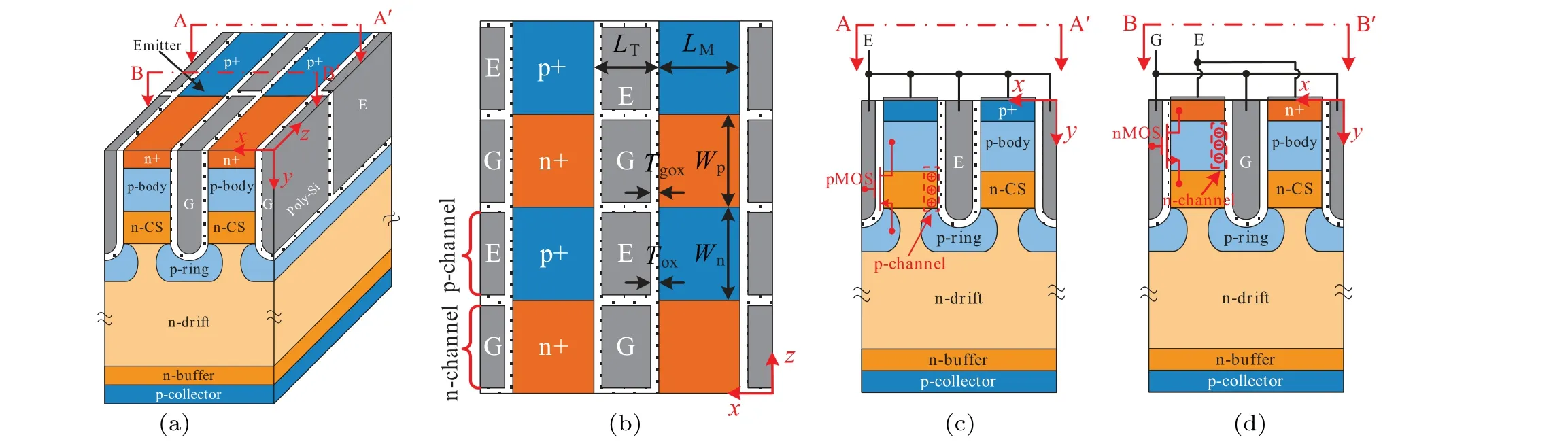
Fig.1.(a)Schematic diagram of proposed IGT IGBT,(b)top view of IGT IGBT,(c)cross-section along cutline AA′,and(d)cross-section along cutline BB′.
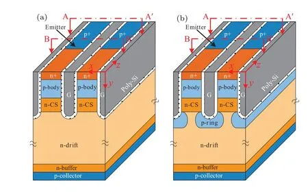
Fig.2.Schematic diagram of(a)CSTBT and(b)p-ring IGBT.
Table 1.Device parameters.
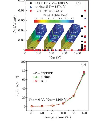
Fig.3.(a)BV characteristics of three IGBT structures,with inset showing electric field distributions of three IGBT structures at breakdown.(b)Comparison of temperature-dependent leakage current among three IGBT structures.
Figure 3(a) shows theBVcharacteristic curves of three IGBT structures.TheBVvalues of all three devices reach values higher than 1300 V.
The inset in Fig.3(a) shows the electric field distributions of the three devices at breakdown.Figure 3(b)compares the curves of leakage current(IL)versus temperature of three IGBT structures.And the leakage current for the IGT IGBT is almost similar to that for the CSTBT and p-ring IGBT.
Figure 4(a) shows the curves ofBVandVonversusNCSfor three IGBT structures.TheBVof CSTBT is lower than
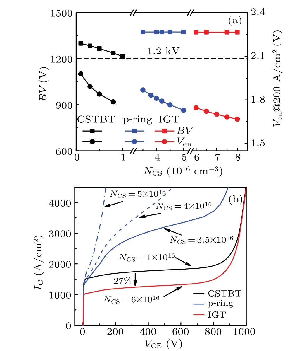
Fig.4.(a) Variations of BV and Von with NCS for three IGBT structures.(b)IC-VCE curves for three IGBT structures with different NCS values(VGE=15 V).
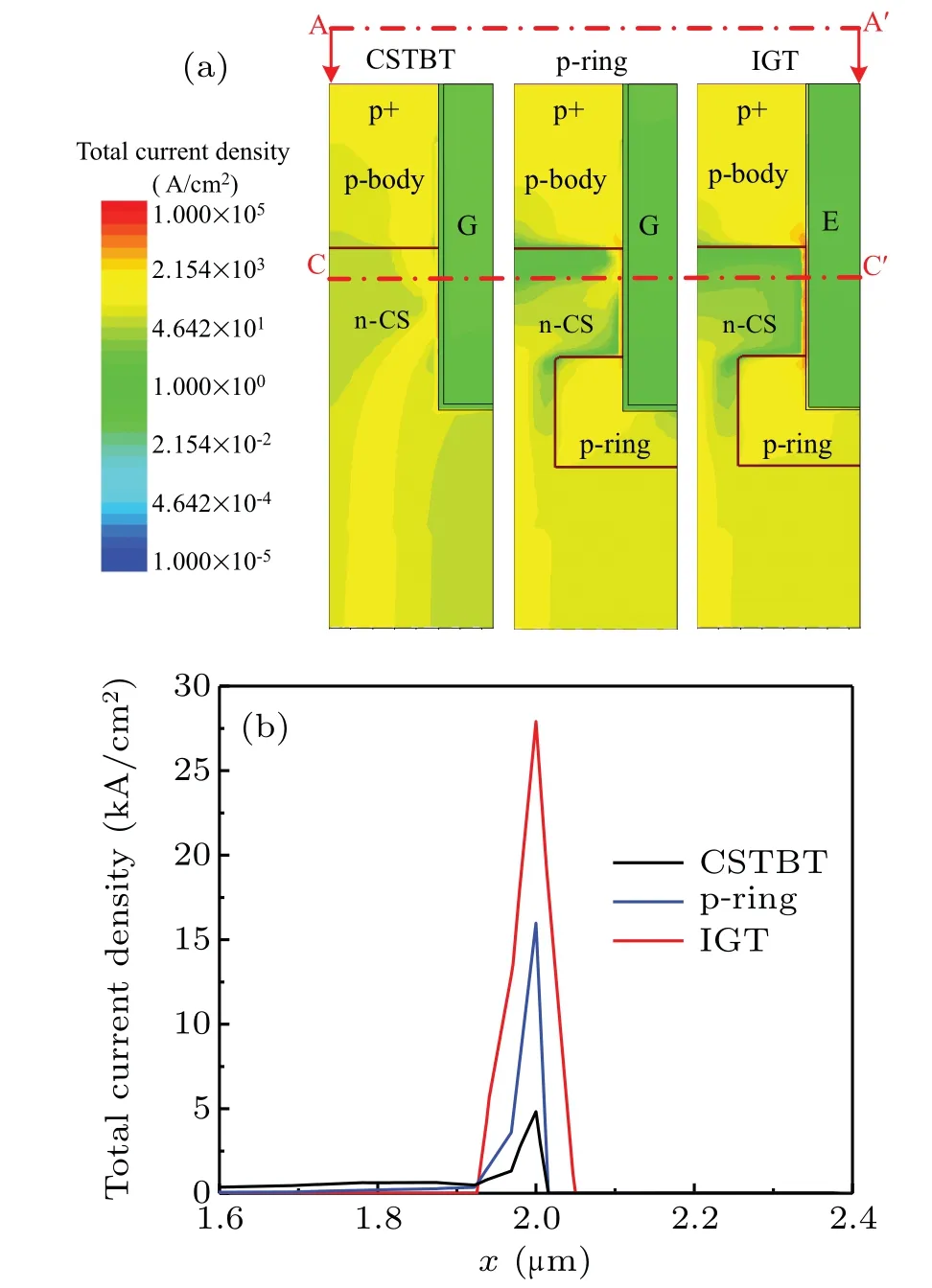
Fig.5.Simulated total current density distributions along (a) cutline AA′and (b) cutline CC′ for three IGBT structures when bus voltage rises to 600 V during turn-off.
Figure 5 shows the total current density distributions along cutline AA′and cutline CC′for three IGBT structures when bus voltage rises to 600 V during turn-off.The current density near the trench of the IGT IGBT is approximately six times higher than that of the CSTBT as shown in Fig.5(b).This means that the built-in p-MOSFET is turned on and provides a p-channel for extracting most of the holes.This reduces the hole current flowing through the main junction.The hole current flowing through the p-channel does not increase the electric field in theydirection.This is because the electric flux emitted from the hole inversion layer ends at the poly emitter in thexdirection.For the IGT IGBT, the extraction of holes by the built-in p-MOSFET alleviates the electric field at the p-body-n-CS junction and suppresses the dynamic avalanche.
Figure 6(a)shows the test circuit for inductive switching.For the IGT IGBT, the built-in p-MOSFET is already turned on before the turn-on moment.A large number of holes injected from p-collector can be extracted through the p-channel quickly.The potential of the p-ring region for the IGT structure shows no sharp increase owing to the absence of hole accumulation therein.Figure 6(b) shows the curves of the potential of the p-ring region below the trench gate andVGEat the turn-on moment.A smallVPof 3.4 V and a small dVP/dtof 11.4 V/μs are obtained in the IGT IGBT.The feature of the IGT IGBT is that its dVP/dtis 60% smaller than that of the p-ring IGBT.Low dVP/dtleads to low dVGE/dt, which further results in low dIC/dt.Thus,a lower dIC/dtand a smaller surge current(Isurge)can be achieved in the IGT IGBT.
Figure 7(a)shows the comparison of capacitance among three IGBT structures.The overlap between gate and collector for the IGT IGBT decreases greatly, thus the gate-tocollector capacitance(CGC)decreases by 67%compared with the counterpart of the CSTBT.In addition,the gate-to-emitter capacitance(CGE)for the IGT IGBT is increased by 34%due to an increase in the overlap between the gate and emitter(Ciss?CGC,soCGEdominates in the input capacitance).Figure 7(b) shows that the gate-to-collector charge (QGC) of the IGT IGBT is 20% that of the CSTBT.All the characteristics are simulated at room temperature unless otherwise stated.
3.Results and discussion
3.1.ON-state voltage
Figure 8 shows the ON-state characteristics for three IGBT structures.TheNCSfor CSTBT,p-ring IGBT,and IGT IGBT is 1×1015cm-3,3.5×1016cm-3,and 6×1016cm-3,respectively.The IGT IGBT obtains the enhanced conductivity modulation caused by increasingNCS.WhenIC=200 A/cm2,theVonat room temperature for IGT IGBT,p-ring IGBT,and CSTBT is 1.75 V,1.87 V,and 1.98 V,respectively.
3.2.Turn-off characteristics
The simulated turn-off characteristics of three IGBT structures as a function of gate resistance (RG) are shown in Fig.9.The CSTBT and p-ring IGBT show a decrease in surge voltage whenRG<5 ?.This indicates the occurrence of DA within the CSTBT and p-ring IGBT.[14]The turn-off curves of IGT IGBT show that surge voltage does not decrease withRGlowering.
Figure 10 shows electric field distributions and impact ionization rate distributions for three IGBT structures when bus voltage rises to 600 V during turn-off.Owing to the increasedNCS, the p-ring IGBT presents significantly higherEmaxand impact ionization rate than the CSTBT.For the IGT IGBT, the electric flux generated by the holes through the pchannel is dispersed in thexdirection.This reduces the vertical electric field and the impact ionization rate at the turn-off moment.Consequently, the maximum impact ionization rate for the IGT IGBT is lowest.
Figure 11(a)shows the turn-off waveforms of three IGBT structures.Both devices are turned off att=52μs.To make a comparison of turn-off loss among three IGBT structures,the turn-off process is divided into two phases as shown in Fig.11(b).The first phase is the voltage rising phase (Evr).TheEvrfor the IGT IGBT(3.5 mJ/cm2)is much smaller than that for the CSTBT(6.7 mJ/cm2)owing to the lower Miller capacitance and the fast extraction of holes caused by self-biased p-channels.The second phase is the current decreasing phase(Ecd).The values ofEcdfor all devices are similar,because of the same carrier lifetime and backside design of IGBTs.
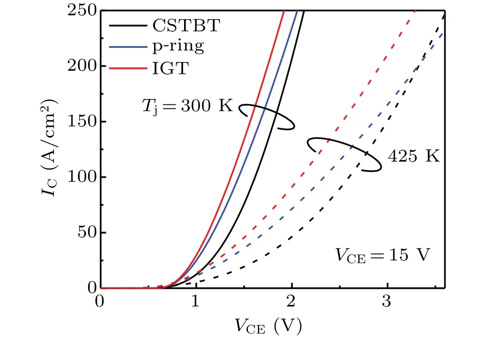
Fig.8.The IC-VCE characteristics of three IGBT structures.
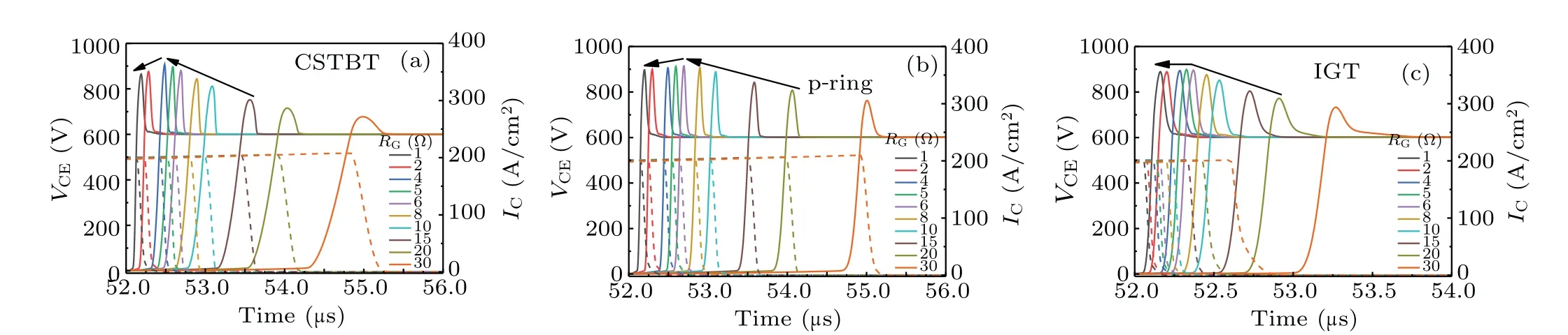
Fig.9.Turn-off characteristics of(a)CSTBT,(b)p-ring IGBT,and(c)IGT IGBT with different values of RG.
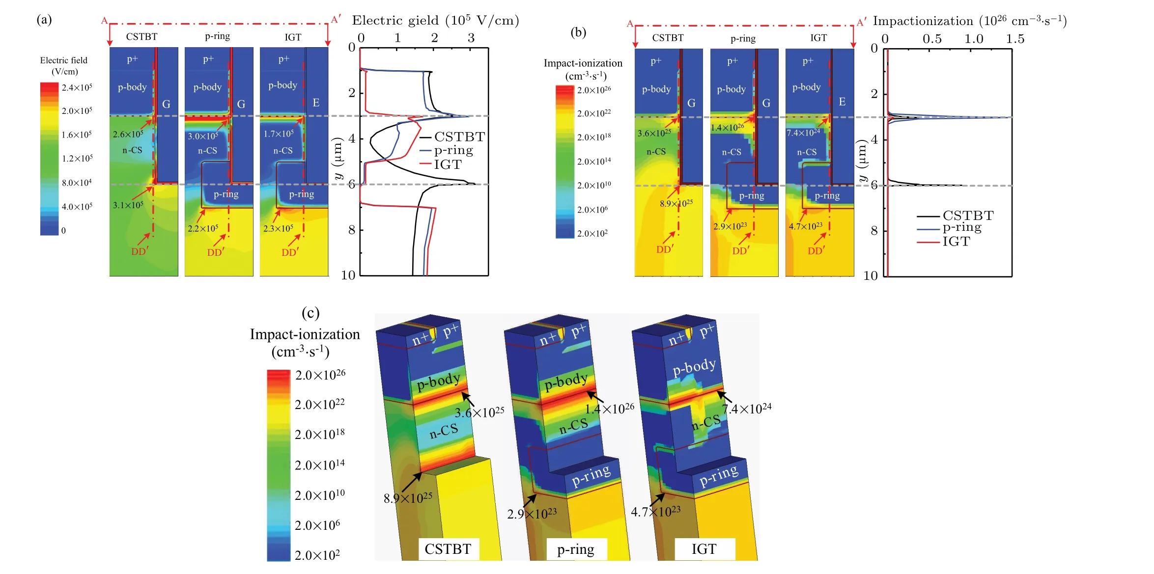
Fig.10.(a) Simulated electric field distributions, (b) simulated impact ionization rate distributions along cutline AA′ and cutline DD′ for three IGBT structures,and(c)simulated impact ionization rate distributions for three IGBT structures,with VCE=600 V and IC=200 A/cm2.
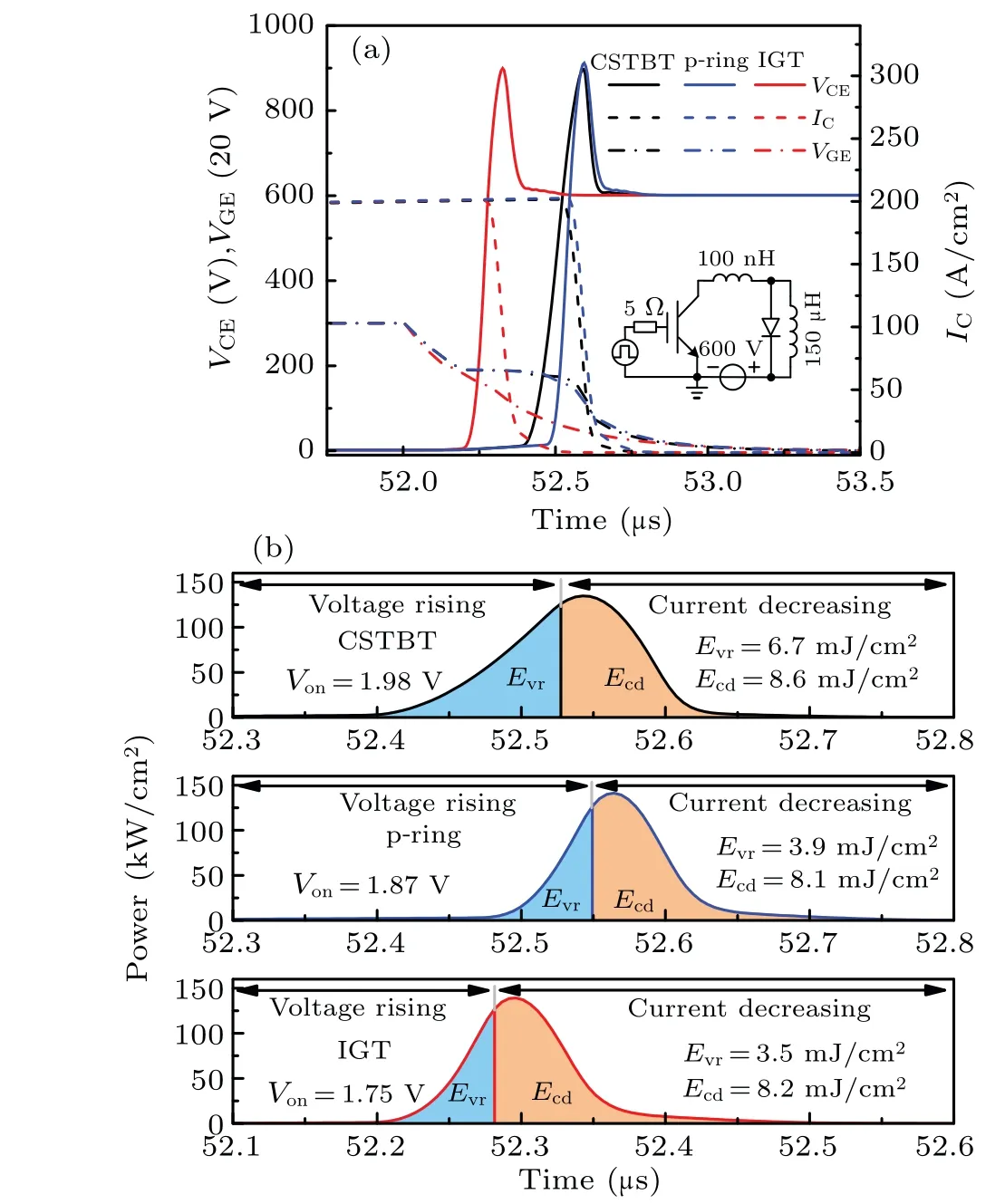
Fig.11.(a)Turn-off waveforms for three IGBT structures and(b)turn-off power analyses for three IGBT structures.
Figure 12 shows that the IGT IGBT has the best trade-off relationship betweenVonandEoff.For the sameVon, theEoffof the IGT IGBT is reduced by 31%compared with that of the CSTBT.This is because of the increasedNCSand the built-in self-biased p-MOSFET.
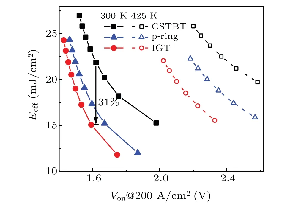
Fig.12.The Von-Eoff trade-off relationships for three IGBT structures.
3.3.Turn-on characteristics
Figure 13 shows the turn-on waveforms of the three IGBTs with different values ofRGunder a small current.The IGT IGBT has lower dIC/dtandIsurgewhen compared with the CSTBT and p-ring IGBT.The IGT IGBT exhibits better controllability ofIsurgeand turn-on dIC/dtthan the CSTBT and p-ring IGBT.Figure 14 shows the influences ofRGon dIC/dtandIsurgeof three IGBT structures.Of the three IGBTs at the sameRGvalue,the IGT IGBT possesses the smallest dIC/dtandIsurge.Figure 14(a)shows that the dIC/dtandIsurgeof the IGT IGBT decrease respectively by 62%and 35%compared with those of the p-ring IGBT, at a current density of 20 A/cm2andRG=20 ?.
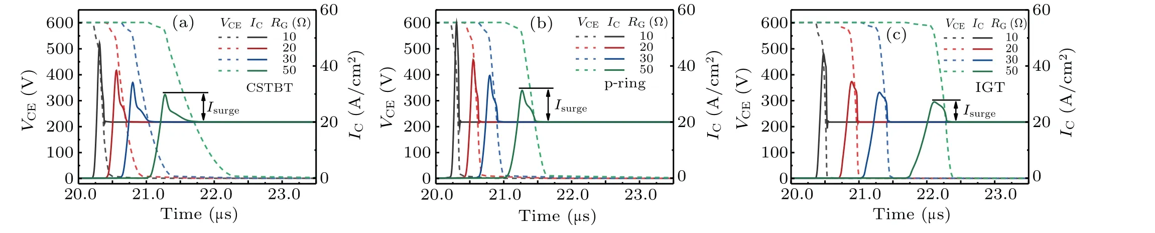
Fig.13.Turn-on characteristics of(a)CSTBT,(b)p-ring IGBT,and(c)IGT IGBT with different values of RG.
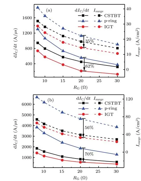
Fig.14.Variations of dIC/dt and Isurge with RG for three IGBT structures at a current density of(a)20 A/cm2 and(b)200 A/cm2.
Figure 15(a)shows the dIC/dt-EonandIsurge-Eontradeoff relationships for the three IGBT structures at a small current density of 20 A/cm2(1/10 rated current).The turn-on losses are calculated underRGvalues of 8 ?, 10 ?, 15 ?,20 ?, and 30 ?, respectively.The IGT IGBT achieves better tradeoff relationships betweenEonand dIC/dt,EonandIsurgethan the CSTBT and p-ring IGBT.For the same value ofEon, the dIC/dtandIsurgeof the IGT IGBT decreases by 52%and 35%compared with those of the CSTBT.At a higher current density of 200 A/cm2, the IGT IGBT still shows the suppressed dIC/dtandIsurgecompared with the CSTBT and p-ring IGBT at the same vale ofEonas shown in Fig.15(b).At a higher current density of 200 A/cm2,the p-ring IGBT has the worst trade-off relationships betweenEonand dIC/dt,EonandIsurge.This is due to the increased self-charging displacement current flowing through the capacitor formed by the p-ring region,the gate oxide and the trench gate.Comparing with the p-ring IGBT,the dIC/dtandIsurgeof the IGT IGBT decrease by 39%and 25%,respectively.
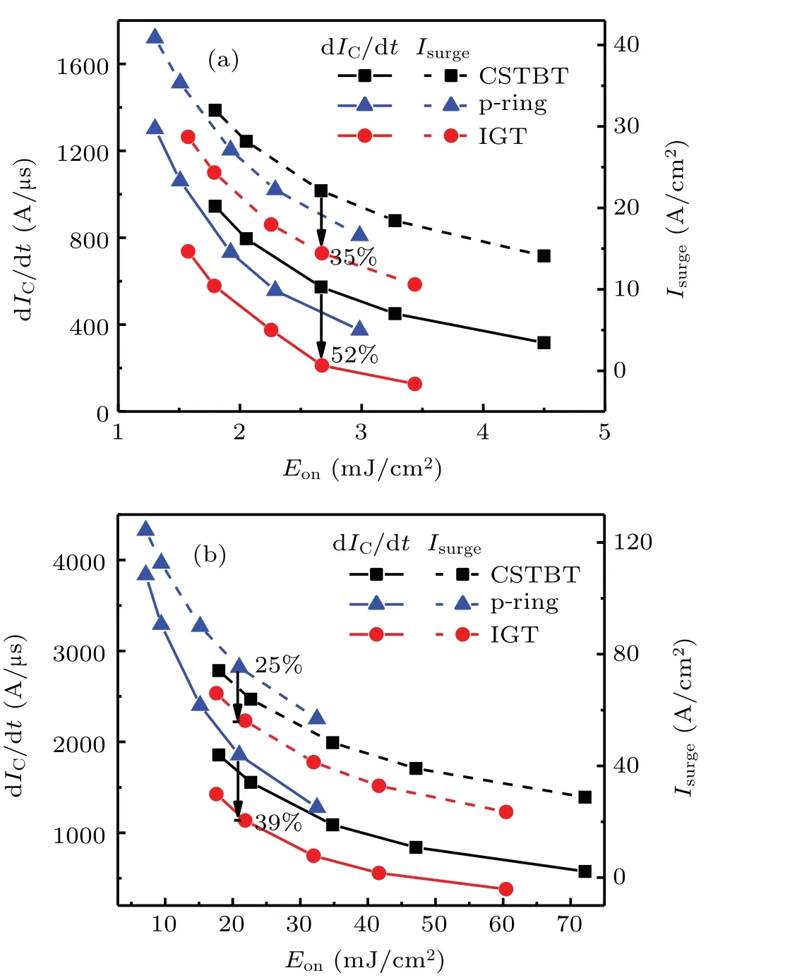
Fig.15.The dIC/dt-Eon and Isurge-Eon trade-off relationships for three IGBT structures at current density of 20 A/cm2 (a)and 200 A/cm2 (b).
4.Fabrication and process
The fabrication process of the proposed IGBT is shown in Fig.16.The p-ring regions are formed by boron implantation at the trench bottom.The trench is then filled with poly-Si.Thereafter,the poly-Si is etched back using a mask.Next,the sidewall oxide is removed,followed by gate oxide growth and poly-Si refilling.Afterwards,the n+region and p+region are formed.Finally, the backside process is carried out and the metal electrodes are formed.
5.Conclusions
An IGBT with interleaved trench-gate is proposed and investigated via numerical analysis.Owing to the interleaved trench gate architecture, the Miller capacitance of the proposed IGBT decreases by 67% compared with that of the CSTBT.The proposed IGT IGBT also shows the improvedVon-Eofftrade-off.Comparing with the CSTBT, theEoffof the proposed IGBT decreases by 31%with the same value ofVon.Furthermore,the proposed IGBT obtains a better turn-on dIC/dtcontrollability and improves the trade-off relationship betweenEonand dIC/dt.For the same value ofEonat a current density of 20 A/cm2,Isurgeand dIC/dtof the proposed IGBT decrease by 35%and 52%compared with those of the CSTBT.
Acknowledgements
Project supported by the Natural Science Foundation of Hunan Province, China (Grant No.2023JJ40161), the Natural Science Foundation of Changsha, China (Grant No.kq2202163), the National Natural Science Foundation of China (Grant No.U21A20499), and the Fundamental Research Funds for the Central Universities, China (Grant No.531118010735).

- Chinese Physics B的其它文章
- Diamond growth in a high temperature and high pressure Fe-Ni-C-Si system: Effect of synthesis pressure
- Si-Ge based vertical tunnel field-effect transistor of junction-less structure with improved sensitivity using dielectric modulation for biosensing applications
- Speeding-up direct implicit particle-in-cell simulations in bounded plasma by obtaining future electric field through explicitly propulsion of particles
- Temperature-induced logical resonance in the Hodgkin-Huxley neuron
- Energy-distributable waterborne acoustic launcher for directional sensing
- Structural stability and ion migration of Li2MnO3 cathode material under high pressures