
Interfacial photoconductivity effect of type-I and type-II Sb2Se3/Si heterojunctions for THz wave modulation
2023-12-02 09:37:36XueQinCao曹雪芹YuanYuanHuang黃媛媛YaYanXi席亞妍ZhenLei雷珍JingWang王靜HaoNanLiu劉昊楠MingJianShi史明堅(jiān)TaoTaoHan韓濤濤MengEnZhang張蒙恩andXinLongXu徐新龍
Chinese Physics B 2023年11期
Xue-Qin Cao(曹雪芹), Yuan-Yuan Huang(黃媛媛), Ya-Yan Xi(席亞妍), Zhen Lei(雷珍), Jing Wang(王靜),Hao-Nan Liu(劉昊楠), Ming-Jian Shi(史明堅(jiān)), Tao-Tao Han(韓濤濤),Meng-En Zhang(張蒙恩), and Xin-Long Xu(徐新龍)
Shaanxi Joint Laboratory of Graphene,State Key Laboratory Incubation Base of Photoelectric Technology and Functional Materials,
International Collaborative Center on Photoelectric Technology,and Nano Functional Materials,Institute of Photonics&Photon-Technology,Northwest University,Xi’an 710069,China
Keywords: photoconductivity,Sb2Se3/Si heterojunctions,THz-TDS,Drude model
1.Introduction
Nobel Prize laureate H.Kroemer once said‘the interface is the device’,since the interface controls the charge transfer,the distribution of quasi-particles and so forth.[1,2]Currently,most studies of interfacial effects and applications usually concentrate on electrical conductivity at interfaces.[3]However,photovoltaic devices and optoelectronic devices are generally utilized under light irradiation, which can be described by the photoconductivity.[4]Hence,a deep comprehensive understanding of the photoconductivity at the interface is necessary to improve the performance of optoelectronic devices.Semiconductor interfaces include three types of heterojunctions according to semiconductor band alignment:[1]type-I,straddling gap; type-II, staggered gap; type-III, broken gap.Transfer and separation of electron–hole pairs between materials are allowed to occur in type-I and type-II heterojunctions, while these processes are hindered in type-III heterojunctions due to the absence of overlapping band gaps.[5,6]Therefore,the study of type-I and type-II heterojunctions currently occupies a key position in the field of optoelectronics.
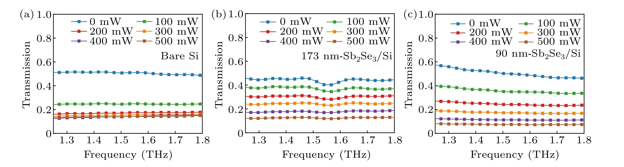
The photoconductivity can be reflected by the photocurrent density, but this method introduces surface impurities and a parasitic effect on the measurement due to the external electrodes.[7,8]Terahertz(THz)time-domain spectroscopy(THz-TDS)provides a non-contact, sensitive and direct measurement of the carrier dynamics,refractive index,carrier conductivity, carrier density and, especially, the interface photoconductivity of semiconductors.[9–11]Since the photoconductivity of materials affects the transmission of THz waves, the THz wave modulation performance is proportional to the photoconductivity at the interface.As such, the photoconductivity of BiFeO3/Si is calculated to be 1.2×10⁴S·m-1and BiFeO3/Si demonstrates a modulation depth of 91.13%.[12]Under 1 W·cm-2illumination,the photoconductivity and photogenerated carrier density of TaS2/Si can reach 380 S·m-1and 5.77×1028cm-3, respectively.[13]However, the mechanism of the influence of type-I and type-II heterojunctions on the photoconductivity and photocarrier density is still unknown.
Antimony selenide(Sb2Se3)possesses a wide adjustable bandgap spanning the range 1.12 eV–1.98 eV,[14,15]allowing for the formation of type-I and type-II heterojunctions with Si.Sb2Se3is nontoxic and inexpensive,[16]and exhibits excellent physical properties such as intrinsic p-type conductivity,[17]a high absorption coefficient(~105cm-1),[18]an excellent carrier density (~1015cm-3)[19]and fast electron trapping.[20]These characteristics make Sb2Se3a promising material for use in solar cells[21–23]and photodetectors.[24,25]In particular,Sb2Se3presents an intriguing interface photoresponse,such as a rise time of 86μs and a fall time of 96μs in type-II Sb2Se3/Si heterojunctions.[25]However, it is still unclear of the interfacial photoconductivity effect between the type-I and type-II Sb2Se3/Si heterojunctions to the THz wave modulation.
Herein,we have prepared 173 nm Sb2Se3/Si(type-I heterojunction)and 90 nm Sb2Se3/Si(type-II heterojunction)and investigated their photoconductivity and photocarrier density via THz-TDS and the Drude model.For THz wave modulation, 173 nm Sb2Se3/Si and 90 nm Sb2Se3/Si demonstrate modulation depths of 49.4% and 62.0%, respectively.Moreover, the type-II heterojunction exhibits a higher photoconductivity and photocarrier density at the interface than the type-I heterojunction.This is because carrier separation is enhanced at the type-II heterojunction interface whereas carrier recombination is enhanced at the type-I heterojunction interface.This work proposes THz-TDS as an effective tool for studying photoconductivity and provides a potential interfacial engineering method to enhance the THz modulation performance.
2.Results and discussion
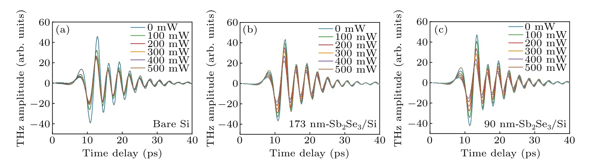
We prepared the Sb2Se3/Si heterojunctions by the physical vapor deposition method.The bandgaps of the 173 nm Sb2Se3and 90 nm Sb2Se3are 1.5 eV and 1.17 eV, respectively.This finding was also reported by Mamtaet al.[14]and Ghoshet al.,[15]indicating that the bandgap decreases as the thickness of Sb2Se3decreases.Detailed descriptions of the sample characterization and experimental setup are given in the supplementary material.Figure 1(a)shows the THz timedomain transmission of the bare Si under continuous wave(CW) laser excitation from 0 mW to 500 mW.It is obvious that the THz amplitudes decrease after passing through the bare Si with increase in CW laser power.This is caused by the change in photoconductivity of the Si under CW laser excitation,[26,27]which further increases the absorption and reflection of the THz wave.The amplitude of THz transmission begins to saturate with CW laser power after exceeding 300 mW.Figures 1(b)and 1(c)present the THz wave transmission of 173 nm Sb2Se3/Si and 90 nm-Sb2Se3/Si under tunable CW laser power.Both heterojunctions present obvious THz wave modulation under CW laser excitation.On the contrary,the THz wave transmission of the bare sapphire substrate and the Sb2Se3/sapphire are both invariable with increasing CW laser power from 0 mW to 500 mW, indicating no effect on THz amplitude modulation,as shown in Figs.S3(a)and S3(b).These results suggest that the photocarriers are not generated in the insulating sapphire substrate under 405 nm CW laser excitation,[28]and the THz absorption of the Sb2Se3film is negligible.As for pure Sb2Se3, photocarriers are generated under above-band-gap(405 nm, 3.06 eV)CW excitation, but the carrier lifetime in Sb2Se3is very short (~35 ps), which further results in negligible photoconductivity change in pure Sb2Se3.[29]Based on above analysis,the THz amplitude modulation is ascribed to the interface response of the Sb2Se3/Si heterojunctions.
In order to further compare the modulation performance of the bare Si, 173 nm Sb2Se3/Si and 90 nm Sb2Se3/Si, we extracted the peak-to-valley values of the THz time-domain amplitude to calculate the modulation depth of the THz wave transmission.We define modulation depth aswhere theTpumpandT0are the THz transmission with and without the CW optical pump, respectively.As can be seen in Figs.2(a)and 2(b),the peak-to-valley values and the modulation depths of the 173 nm Sb2Se3/Si and 90 nm Sb2Se3/Si both show linear dependences on the CW pump power,while the peak-to-valley value and the modulation depth of the bare Si show a saturation dependence on the CW laser power and saturate at 300 mW.For bare Si, this saturation is due to the electrostatic field screening formed by the accumulation of holes on the surface.[30,31]According to the surface band bending of bare Si shown in Fig.S4, under CW illumination the electrons and holes are separated by a surface built-in electric field, then the electrons move into the Si and the holes move towards the surface.This movement consequently enhances the photocarrier density and THz absorption.The bare Si, 173 nm Sb2Se3/Si and 90 nm Sb2Se3/Si present modulation depths of 49.3%, 49.4% and 62.0%, respectively.The 90 nm Sb2Se3/Si heterojunction has a larger modulation depth than bare Si.This can be explained by the transport of photogenerated carriers at the Sb2Se3/Si interface,which leads to the enhanced modulation of THz amplitude in the Sb2Se3/Si heterojunction.Since the Sb2Se3layer will absorb the incident light when passing through Sb2Se3,the transmitted optical power at the Sb2Se3/Si interface is low and the small number of photocarriers are unable to form a large built-in interfacial field under a low excitation power.When the excitation power increases to 500 mW, according to the Beer–Lambert law,I=I0e-α0l[whereI0, e,α0andlare intensity of laser excitation, the natural index, absorption coefficient (~0.3 @405 nm[32])and sample thickness,respectively],the transmitted optical power at the Sb2Se3/Si interface is calculated to be as high as~450 mW.Hence,a large built-in electric field can be formed at the interface,which accelerates the separation of photocarriers and prolongs the photocarrier lifetime,resulting in a significant enhancement of THz modulation.
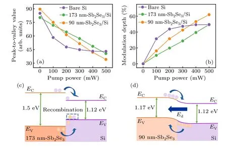
Fig.2.Transmitted THz time-domain amplitudes of (a) peak-to-valley value and (b) modulation depth of bare Si (purple), 173 nm Sb2Se3/Si(green), and 90 nm Sb2Se3/Si (orange) with CW laser power ranging from 0 mW to 500 mW.Band alignment of (c) 173 nm Sb2Se3/Si and(d)90 nm Sb2Se3/Si under CW light illumination.
Based on the above analysis, the THz amplitude modulation is ascribed to the interface response of the Sb2Se3/Si heterojunctions according to their band alignments,as we will now discuss.Based on the bandgap of Sb2Se3with different thicknesses (Figs.S2(b) and S2(d)), 173 nm Sb2Se3/Si and 90 nm Sb2Se3/Si form type-I and type-II heterojunctions, respectively.[14,15]As shown in Fig.2(c), for 173 nm Sb2Se3/Si,the electrons and holes would both transport to the Si due to the band alignment of the type-I heterojunction.[1]On the one hand, the simultaneous transfer of electrons and holes to Si will enhance the recombination of photocarriers and reduce the concentration of photogenerated carriers.[33]This property presents promising potential in light-emitting devices.[1]On the other hand, the photoconductivity of Si is described as[13,34]σ=e(neμe+nhμh),where thenh(ne)andμh (μe) represent the carrier density and mobility of holes(electrons), respectively.Since Si is an n-type semiconductor, its photoconductivity is mainly determined by the electrons.For 173 nm Sb2Se3/Si, the mobility of the photocarrier in Si (1400 cm2·V-1·S-1) is larger than that in Sb2Se3(14.2 cm2·V-1·S-1),[35] and the effect of Sb2Se3 on the photoconductivity of the Sb2Se3/Si heterojunction is negligible.This is the reason why the THz wave modulation depth of 173 nm Sb2Se3/Si is comparable to that of bare Si under 500 mW excitation.For 90 nm Sb2Se3/Si, due to the band alignment of the type-II heterojunction,[1]the electrons would transport to the Si and the holes would transport to the Sb2Se3.This consequently forms a large internal electric field (Ed) at the 90 nm Sb2Se3/Si interface, which reduces the recombination of photogenerated carriers,thereby prolonging the carrier lifetime and increasing the carrier concentration.Hence,90 nm Sb2Se3/Si has a greater modulation depth than bare Si and 173 nm Sb2Se3/Si.
Since the plasmon model[39]and quantum plasmon model[40]are suitable for micro/nanostructural materials with sizes smaller than the THz wavelength the damped harmonic oscillator and scattering rates should be considered.However, the size of continuous multilayer Sb2Se3films is larger than the THz wavelength,which makes the samples similar to bulk materials (e.g., bulk Si).The photoconductivity of bulk Si (above 0.4 THz) is also consistent with the Drude model.Thus, herein, we have utilized the Drude model to describe the photoconductivity as[12]σ(?ω)=(γω2p
)/(π(ω2+γ2)),whereis the plasma frequency (N,e,ε0andmrepresent the photocarrier density, electronic charge,free-space permittivity and carrier effective mass, respectively)andγis the damping coefficient.Hence,the photocarrier density is described asN=σ(?ω)(ω2+γ2)ε0mπ/(γe2).Based on the Drude model and Figs.4(a)–4(c), the extracted photocarrier densities of bare Si,173 nm Sb2Se3/Si,and 90 nm Sb2Se3/Si increase significantly with increasing CW power,as shown in Figs.4(d)–4(f).Herein, the photoconductivity and photocarrier density are directly correlated,thus THz wave absorption will be enhanced under a high photocarrier density,resulting in a high modulation depth.According to the values at 1.8 THz,the photocarrier density of 173 nm Sb2Se3/Si(0.8×1015cm-3) is~1.1 times larger than that of bare Si(0.7×1015cm-3), while the photocarrier density of 90 nm Sb2Se3/Si(1.5×1015cm-3)is about twice that of bare Si under 500 mW excitation(see detailed comparison in Fig.S6(b)).These results demonstrate that a type-II heterojunction is better than a type-I heterojunction for THz modulation performance.The recombination between electrons and holes causes a slight change in photoconductivity for the type-I Sb2Se3/Si heterojunction, while the separation of electrons and holes leads to a great change in photoconductivity for the type-II Sb2Se3/Si heterojunction.[41]
3.Conclusion
In summary, we have prepared 173 nm Sb2Se3/Si (type-I)and 90 nm Sb2Se3/Si(type-II)heterojunctions based on the thickness-dependent-bandgap properties of Sb2Se3.Concerning their THz modulation performance,the modulation depths of bare Si,173 nm Sb2Se3/Si and 90 nm Sb2Se3/Si are 49.3%,49.4% and 62.0%, respectively.The photocarrier density of 90 nm Sb2Se3/Si (1.5×1015cm-3) is about twice that of bare Si, while the photocarrier density of 173 nm Sb2Se3/Si(0.8×1015cm-3) is~1.1 times higher than that of bare Si(0.7×1015cm-3).These results are ascribed to the interfacial photoconductivity effect, since the type-I heterojunction accelerates carrier recombination and the type-II heterojunction accelerates carrier separation.Our work deepens our understanding of interface physics that is beneficial for improving the photoelectronic response at the interface of photoelectronic devices,such as solar cells and photodetectors.We have also unveiled the interfacial photoconductivity effect, including the photocarrier lifetime, the separation of electrons and holes and the interfacial electric field,which could provide the physical basis for highly effective THz modulators.
Acknowledgment
Project supported by the National Natural Science Foundation of China (Grant Nos.12261141662, 12074311, and 12004310).

- Chinese Physics B的其它文章
- The application of quantum coherence as a resource
- Special breathing structures induced by bright solitons collision in a binary dipolar Bose–Einstein condensates
- Effect of short-term plasticity on working memory
- Directional-to-random transition of cell cluster migration
- Effect of mono-/divalent metal ions on the conductivity characteristics of DNA solutions transferring through a microfluidic channel
- Off-diagonal approach to the exact solution of quantum integrable systems