
Facile integration of an Al-rich Al1-xInxN photodetector on free-standing GaN by radio-frequency magnetron sputtering
2023-12-02 09:29:36XinkeLiu劉新科ZhichenLin林之晨YuhengLin林鈺恒JianjinChen陳建金PingZou鄒蘋JieZhou周杰BoLi李博LonghaiShen沈龍海DeliangZhu朱德亮QiangLiu劉強WenjieYu俞文杰XiaohuaLi黎曉華HongGu顧泓XinzhongWang王新中andShuangwuHuang黃雙武
Chinese Physics B 2023年11期
Xinke Liu(劉新科), Zhichen Lin(林之晨), Yuheng Lin(林鈺恒), Jianjin Chen(陳建金),Ping Zou(鄒蘋), Jie Zhou(周杰), Bo Li(李博), Longhai Shen(沈龍海),Deliang Zhu(朱德亮), Qiang Liu(劉強), Wenjie Yu(俞文杰), Xiaohua Li(黎曉華),Hong Gu(顧泓), Xinzhong Wang(王新中), and Shuangwu Huang(黃雙武),?
1College of Materials Science and Engineering,Institute of Microelectronics(IME),Guangdong Research Center for Interfacial Engineering of Functional Materials,Shenzhen University,Shenzhen 518060,China
2School of Science,Shenyang Ligong University,Shenyang 110159,China
3State Key Laboratory of Functional Materials for Informatics,Shanghai Institute of Microsystem and Information Technology,Chinese Academy of Sciences,Shanghai 200050,China
4Gusu Laboratory of Materials Science,Suzhou 215123,China
5Information Technology Research Institute,Shenzhen Institute of Information Technology,Shenzhen 518172,China
Keywords: Al1-xInxN,photodetector,GaN,radio-frequency magnetron sputtering,ternary alloy
1.Introduction
III-nitride semiconductor material has been intensively applied in optoelectronic and electronic devices because of its exceptional physical and chemical properties, especially its excellent photoelectric properties.[1–3]In particular,Al1-xInxN is considered to be a powerful candidate material for optical and electronic devices.The band gap of Al1-xInxN can be tuned from 0.7 eV (InN) to 6.2 eV (AlN) by adjusting the Al/In ratio, thereby covering an unprecedented spectral range in the ultraviolet and infrared bands,making it feasible to select a cut-off wavelength for a single-wave segment or multi-wave segment photodetector.[4–6]Extensive research on Al1-xInxN has been carried out since 2000, but it is difficult to grow, making it the least attractive material among the ternary nitride alloys.The growth process of Al1-xInxN ternary alloys involves multi-alloy phases of different compositions and structures, and the unintentional doping of nitrogen vacancies can seriously affect the photoresponsivity of any photodetector.[7]Therefore, it is crucial to research the fabrication of high-performance ternary alloy Al1-xInxN material.To develop a high-performance Al1-xInxN visible-light photodetector, substrate selection is also essential.A low degree of lattice mismatch between Al-rich Al1-xInxN and GaN makes it easier to obtain single-phase Al1-xInxN.Theoretically,a two-dimensional electron gas will be generated at the GaN interface in the Al1-xInxN/GaN heterostructure, providing both a high carrier density and high mobility.[8–15]One of the main disadvantages of ternary nitride synthesis is the challenge of solid solution between the binary compounds, i.e.,GaN, AlN and InN.The synthesis of Al1-xInxN alloys using molecular beam epitaxy or metal-organic vapor phase epitaxy requires very high temperatures and there are often phase separation effects.In comparison,radio-frequency magnetron sputtering (RF-MS) permits the preparation of Al1-xInxN at low temperatures and allows for a non-toxic reaction, mass production and the deposition of single-phase Al1-xInxN over large areas.[16–18]Currently, an exciting route for fabricating photodetectors is to deposit Al1-xInxN film on a GaN substrate by RF-MS.[5,19]
In this work, we successfully fabricated an Al1-xInxN/GaN visible-light photodetector by direct RF-MS.The Al1-xInxN/GaN sample was characterized by scanning electron microscopy(SEM),x-ray photoelectron spectroscopy(XPS),x-ray diffraction(XRD)and UV–visible spectroscopy to evaluate its chemical composition,crystallinity and optical properties.These represent the quality of the Al1-xInxN used in the photodetector described in the remainder of this paper.Next,the Al1-xInxN/GaN photodetector was characterized by theI–Vcurve,spectral responsivity and response time in order to evaluate the device quality.
2.Experimental details
Al1-xInxN films were grown directly on a free-standing GaN substrate by RF-MS,and the sputtering target was composed of a sheet of In metal(99.999%purity)attached to the surface of the Al target(99.999%purity).A schematic of the deposition chamber is shown in Fig.1(a).Firstly,the substrate and Al target were ultrasonically cleaned in anhydrous ethanol for 20 min and blown dry with nitrogen.Then, the substrate and the In/Al target were placed in the deposition system.The reaction chamber has two parallel electrodes: the upper one was assigned as the cathode and substrate support while the lower one was the anode and mounting gear of the In/Al target.The anode is connected to the water-cooling system.Preconditioning of the substrate surface was performed with Ar plasma (DC bias 300 V) at a chamber pressure of 30 Pa for 15 min to activate the surface bonds.Next,the reaction chamber was vacuumed to 5×10⁻⁴Pa under 1 Pa chamber pressure and 300 W RF power,and the target was splashed in the argon plasma for 10 min with the aim of removing contaminants.Meanwhile,the chamber pressure was 1 Pa,the Ar:N2flow ratio was 60:40, the deposition time was 1 h, the substrate temperature was 350?C and the distance between the substrate and target was 7 cm.Finally, fork finger electrodes of Ni(20 nm)/Au(50 nm)were prepared on Al1-xInxN/GaN using UV lithography and electron-beam evaporation.
The thickness of the Supra 55 sapphire was measured by SEM.The XRD curve was measured by a D8 Advance to calculate the structures, elements, chemical states and morphologies of the films.XPS spectra were taken by a 220 VG ESCALABi-XL system with a constant energy source of 20 eV, C 1s (284.6 eV) was used for calibration and monochromatic AlKα(1486.6 eV) was the x-ray source.A UV–visible spectrometer (Shimadza-2450, Tokyo, Japan)was used to characterize the absorbance of the films in the range of 300–800 nm.The electrical characteristics of the Al1-xInxN/GaN photodetector were studied with a Keithley 4200-SCS semiconductor parameter analyzer (Keithley,Beaverton, OR, USA).All measurements were carried out at room temperature.
3.Results and discussion
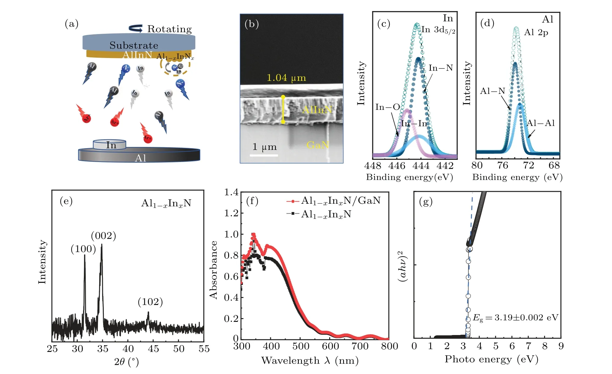
Figure 1(a)shows a schematic diagram of the principle of the Al1-xInxN film deposition process.The combined probability of targeting Al and In with nitrogen is almost consistent with the sputtering path;the sputtering yield of the target material was changed by designing the ratio of the Al/In target material.Herein we have fabricated Al-rich Al1-xInxN film.The SEM image in Fig.1(b) shows a highly compact Al1-xInxN layer on a thick GaN base layer with a thickness of about 1.04μm.It can be seen that the grown layer has no cracks and exhibits good adhesion.
The elemental composition and chemical composition of Al1-xInxN were further understood by XPS analysis.Figures 1(c) and 1(d) show the Al 2p and In 3d5/2core-level spectra, respectively.As a binding energy reference, the C 1s peak from contaminating carbon is set at 284.6 eV.The corresponding Al 2p core-level photoelectron spectrum is deconvoluted into two main components at 73.92±0.1 eV and 73.21±0.1 eV, which are assigned to Al–N and Al–Al bonds, respectively.The In3d5/2core-level spectrum of the Al1-xInxN sample is deconvoluted into three main sub-peaks centered at 444.15±0.1 eV, 444.21±0.1 eV and 445.15±0.1 eV, which are attributed to In–In, In–N and In–O bonds,respectively,with the In–N sub-peak being the most dominant.These results are consistent with previous studies which confirmed the formation of an Al1-xInxN layer.[20,21]However, the appearance of In–O bonds is possibly due to the formation of a thin oxide layer on the surface of the Al1-xInxN.The Al–Al and In–In bond components are attributed to a higher concentration of active In and Al atoms reaching the growth sites compared with active N atoms at this temperature.[22–24]
Figure 1(e) depicts the XRD pattern of the as-prepared Al1-xInxN, and the observed diffraction peaks correspond to(100), (002) and (102) planes of wurtzite Al1-xInxN.In particular,the phases of Al,In and AlN and InN are not observed,indicating any phase separation in the sample.Based on the position of the (100) and (002) peaks of Al1-xInxN, we can calculate the lattice parameters of the samples.The lattice constantsaandcfor Al1-xInxN are determined as 2.83 ?A and 5.16 ?A,respectively.The crystallite size of Al1-xInxN is calculated from the(002)peak according to Scherrer’s equation,D=0.89λ/βcosθ,[25]and the crystallite sizeDis 12.52 nm.The alloy composition Al1-xInxN along the(002)plane is calculated using Vegard’s law and Vegard’s rule that all growing films are supposed to be pressure-free,as shown below:[7]
In Eq.(1), the lattice constants of Al1-xInxN, AlN (4.982 ?A)and InN (5.703 ?A) are represented byCAlInN,CAlNandCInN,respectively.The result concerning the In contentxfor Al1-xInxN is 0.25.Due to the low symmetry of the hexagonal wurtzite crystal structure, the positive and negative ions that deviate from the inside of the crystal produce dipole moments,causing ion polarization.Polarization has an important influence on the photoelectric properties of materials.[26,27]To further investigate the optical properties of Al1-xInxN,the absorbance of Al1-xInxN/GaN heterostructures was measured, as shown in Fig.1(f).It can be observed that the absorbance of the Al1-xInxN/GaN heterostructures has significantly improved compared with that of Al1-xInxN, which can be attributed to the polarized charges at the interface further strengthening the electron–phonon coupling between Al1-xInxN and GaN.In addition,the exciton energy generated in Al1-xInxN is mainly dissipated by the lattice vibration in the adjacent GaN substrate,which leads to a shortened exciton life.[28]Through the polarization effect between Al1-xInxN and GaN,the energy structure of Al1-xInxN is adjusted to improve the light absorption capacity.Noticed that the most substantial absorbance peak of Al1-xInxN emerges at~340 nm in Fig.1(f).The incident wavelength interval of 300–400 nm has higher absorbance, and two excitation absorption peaks appear.There are no significant absorption peaks above 400 nm for Al1-xInxN/GaN.Therefore, a 365 nm wavelength light source was used in the following device tests.Thus, the absorption rate of Al1-xInxN can be defined asμ=1-1/10θ.Note thatθ=log10(I0/It),whereI0andItare the intensities of the incident and transmitted light,respectively.[29]The apparent optical band-gap energy (Eg) is obtained by linear fitting the squared absorption coefficient as a function of the light quantum in the Tauc plot(in Fig.1(g)).Light scattering as well as reflection loss are ignored here.[2,19]The equation is[30]
whereCis an energy-independent constant and another constantmis called the power factor of the transition mode Al0.75In0.25N.For a direct band-gap semiconductor like Al1-xInxN alloym= 1/2.Figure 1(g) shows the relationship between the absorption coefficientaand the incident light quantumhνof the Al1-xInxN on GaN.The energy of the optical band gap is calculated according to the absorption spectrum by Tauc’s law,and the result is 3.19 eV.[31]
Further energy level alignment characterization of Al0.75In0.25N and GaN was done by XPS combined with energy band theory.XPS has been proven to be an efficient way to determine the band offset at a heterojunction interface.[32,33]In order to determine the valence band offset (VBO) of the Al0.75In0.25N/GaN interface, the Al 2p and Ga 2d core-level spectra were employed for the Al0.75In0.25N and GaN materials, respectively.As shown in Figs.2(a) and 2(b), the following formulae can be used to calculate the VBO ?Evand conduction band offset ?Ecof Al0.75In0.25N and GaN:[34]
The vacuum level is taken as the forward reference.Obviously, the Al0.75In0.25N/GaN system has a type II alignment in Fig.2(c).Under UV irradiation,interlayer transitions may occur at the lowest part of the conduction band and the highest part of the valence band and the charge separation of photoinduced carriers can reduce charge recombination, which also indicates that the device may show excellent performance in optoelectronic devices.Therefore, a Al0.75In0.25N/GaN photodetector was prepared to demonstrate the ability to detect light.

Figure 3(a)shows a three-dimensional schematic view of an Al0.75In0.25N photodetector fabricated on a GaN substrate.Figure 3(b)shows one of the electrodes of the transparent array.The two fork-shaped interdigital contacts consist of Au(50 nm)/Ni(20 nm),the separation of the finger gaps is 18μm and the effective area is 4.82 μm2.The current–voltage (I–V) curves of the device at different laser incident powers for a single wavelength of 365 nm are used to further analyze the critical parameters of the photodetector.
TheI–Vcurves of devices with different incident powers and voltages were increased from-20 V to 20 V.The measuredI–Vcurves are shown in Fig.3(c); it can be observed thatIlightincreases as the power increases.This phenomenon is attributed to the role of photoinduced carriers generated by the device under laser irradiation.To quantify the photosensitive performance of the photodetector, the photocurrentIphis defined as[35]
In Eq.(6),Idarkis the current in dark conditions andIlightis the current under light irradiation.Significantly, the device still shows high photocurrent at a low incident power of 2.0163 μW, indicating strong low-light detection capability.Figure 3(d)shows the extractedIphplotted as a function of the effective power (P) irradiated under a wavelength of 365 nm at a bias voltage of 20 V.The upward trend ofIphslowed down whenP>4.5 μW.As reported in previous literature,[36]this phenomenon can be attributed to the light saturation of absorption and the trapping of electrons and holes due to the existence of defects and charge impurities.
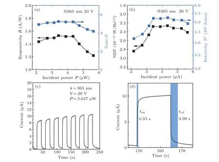
Figure 4(a)shows the photoresponsivityRand photoconductive gainGof the fabricated device as a function of the effective power at 365 nm wavelength under a bias voltage of 20 V.Ris a significant parameter in the performance of photodetectors,and can quantify the spectral and frequency characteristics of photoconversion.Ris calculated by[37]
whereIphis extracted from Eq.(6),SandPiare the area of active regions of the device and power density of the incident laser irradiation,respectively.The photoconductivity gainGis defined as the number of photogenerated carriers that are generated from unit photons, and is another important parameter for the evaluation of a photodetector.It is calculated by[37]
wherePabsis the absorbed power, which is defined asPabs=μPi, withμthe absorption percentage calculated above andPinthe incident power,his Plank’s constant,vis the frequency of the incident laser andqis the elementary charge.[42]With increasing incident power, bothRandGshow a trend of first rising and then decreasing.The Al0.75In0.25N/GaN photodetector has the highest responsivity of 1.52 A·W-1at an incident laser power is 3.425μW,andGalso reaches its maximum value at the same power.This phenomenon can be explained by the saturation of the defect state at the interface and the low carrier recombination frequency under a low-power laser as well as the long carrier lifetime.[29]To further discuss the performance of the Al0.75In0.25N photodetector we calculated the noise equivalent power (NEP) and the normalized detection rate (D*) at different incident powers at a wavelength of 365 nm in Fig.4(b).The NEP can quantify the detection capability of the photodetector,with a smaller NEP indicating a higher sensitivity.The NEP can be calculated as follows:[38]
whereRis obtained from Eq.(7) and ?fis the bandwidth.Usually, the dark current makes the major contribution, and causes scattering noise, Johnson–Nyquist noise and flicker noise.The parameterD*contributes to quantifying the signal detected by the photodetector.D*can be calculated as follows:[38]
whereAis the effective area of the Al1-xInxN under the laser irradiation conditions.The NEP can be extracted from Eq.(10).As shown in Fig.4(b), the lowest NEP value is 2.26×10⁻¹³W·Hz-1/2and the highestD*value is 9.61×10⁸Jones calculated for the Al1-xInxN photodetector at 365 nm laser wavelength and 20 V bias.
Figure 4(c) shows the periodic flow over time of the Al1-xInxN/GaN photodetector under a continuous light pulse.The pulsed light is set to be on or off every 10 s under the 365 nm laser (5.647 μW) and 20 V bias.We can see that the device has a relatively stable switching characteristic.The rise time (trise) from the dark signal to 90% of the maximum signal upon illumination and the fall time (tfall) to 10%are commonly used to characterize the temporal response of a photodetector.As shown in Fig.4(d), the calculatedtriseandtfallfor the Al1-xInxN/GaN photodetector are 0.55 s and 3.99 s, respectively.The Al1-xInxN photodetector based on a GaN substrate achieves a fast photoresponse, and benefits from the formation of a two-dimensional electron gas at the Al1-xInxN/GaN heterojunction interface and the polarization effect.However, the device shows a long decay time after the optical stimulus has been removed;one of the reasons for this is that Al1-xInxN is associated with punctate impurities and defects in the substrate.[40]To emphasize the advances achieved with the Al1-xInxN/GaN photodetector a comparison of the results of several studies on the photoresponsivity properties of Al1-xInxN photodetectors is summarized in Table 1.Compared with other devices,our Al1-xInxN/GaN device has a higher photoresponsivity and specific detectivity,and the device achieves a fast photoresponse due to the introduction of the GaN substrate.

Photodetector R(A/W) Dark current(A) D* (Jone) Response time(s) Year Ref.AlInN/GaN 1.5296 4.09×10⁻⁷ 9.61×10⁸ 0.55 2022 this work AlInN/Si0.47– – –2018[41]AlN/sapphire 0.6×10⁻³ 2.41×10⁻¹² – 0.9 2020 [42]Al0.33In0.67N/glass 1.26×10⁻⁴ – 1.2×10⁵ 1.39 2022 [7]Al0.58In0.42N/GaAs0.06––0.72016[43]GaN/sapphire0.633– – –2018[44]
4.Conclusion
In summary, this study has successfully demonstrated an Al1-xInxN/GaN photodetector with low dark current,high photoresponsivity and fast response speed fabricated using the RF-MS deposition method and simple semiconductor fabrication methods.The Al1-xInxN alloy film was successfully prepared with good crystallinity and homogeneity measured by SEM and XPS core-level spectra.The alloy composition of Al1-xInxN was then analyzed by XRD, andx=0.25 was calculated.Calculation of the absorbance of the film gave the band gap of Al0.75In0.25N as about 3.19 eV.In addition,the polarization effect of the III-nitride heterostructure has a positive impact on improving the absorption capacity of Al1-xInxN.The electron transport behavior of the Al1-xInxN/GaN heterojunction was further proved by XPS valence band spectroscopy.Subsequently, a Al0.75In0.25N photodetector was prepared, showing excellent performance with a maximum photoresponsivity of 1.52 A·W-1and time to reach maximum photocurrent of 0.55 s under 365 nm laser illumination.Table 1 compared various photodetectors with the one reported in this work.In recent years there have been few reports on Al1-xInxN alloy,and we have achieved unprecedented performance by controllable fabrication of Al1-xInxN via physical vapor deposition technology to fabricate a photodetector on GaN substrate.
Acknowledgements
Project supported by the National Natural Science Foundation of China (Grant Nos.61974144, 62004127, and 12074263), Key-Area Research and Development Program of Guangdong Province (Grant Nos.2020B010174003 and 2020B010169001), Guangdong Science Foundation for Distinguished Young Scholars (Grant No.2022B1515020073),the Science and Technology Foundation of Shenzhen (Grant No.JSGG20191129114216474), and the Open Project of State Key Laboratory of Functional Materials for Informatics.
猜你喜歡
Plasma Science and Technology(2024年2期)2024-03-19 02:36:52
Chinese Physics B(2023年9期)2023-10-11 07:56:42
電腦知識與技術(2022年11期)2022-05-31 00:28:57
電腦知識與技術(2022年9期)2022-05-10 14:58:45
知音海外版(下半月)(2020年3期)2020-12-24 10:48:29
考試與評價·八年級版(2020年3期)2020-11-02 02:39:24
Journal of Donghua University(English Edition)(2020年6期)2020-02-01 08:56:12
Journal of Oceanology and Limnology(2018年2期)2018-05-07 06:07:52
小學生學習指導(高年級)(2017年4期)2017-03-08 08:24:31
Journal of Meteorological Research(2014年4期)2014-12-14 06:57:57

- Chinese Physics B的其它文章
- The application of quantum coherence as a resource
- Special breathing structures induced by bright solitons collision in a binary dipolar Bose–Einstein condensates
- Effect of short-term plasticity on working memory
- Directional-to-random transition of cell cluster migration
- Effect of mono-/divalent metal ions on the conductivity characteristics of DNA solutions transferring through a microfluidic channel
- Off-diagonal approach to the exact solution of quantum integrable systems