
Novel double channel reverse conducting GaN HEMT with an integrated MOS-channel diode
2023-10-11 07:56:36XintongXie謝欣桐ChengZhang張成ZhijiaZhao趙智家JieWei魏杰XiaorongLuo羅小蓉andBoZhang張波
Chinese Physics B 2023年9期
Xintong Xie(謝欣桐), Cheng Zhang(張成), Zhijia Zhao(趙智家), Jie Wei(魏杰),Xiaorong Luo(羅小蓉), and Bo Zhang(張波)
School of Electronic Science and Engineering,University of Electronic Science and Technology of China,Chengdu 610054,China
Keywords: AlGaN/GaN,HEMT,double-channel,reverse conduction
1.Introduction
GaN-based power devices are promising candidates for next-generation power switching applications owing to their superior device properties, including low specific onresistance (Ron,sp), low switching loss, and high breakdown voltage (BV).[1–4]In many power switching circuits such as DC–AC inverters and boost converters, low-loss reverse conduction of the power transistors is required to provide a freewheeling current path so that the inductive load current would not be disrupted and high voltage peaks are suppressed.[5]
The conventional GaN HEMT itself can reversely conduct, and its reverse turn-on voltage (VRT) depends on the gate–source bias (VGS) and threshold voltage (Vth) (VRT=|Vth-VGS|).[6–8]In practical power switching applications,VRTwould even further increase since a negativeVGSis often employed to prevent false turn-on and increase noise immunity.[9]An externally anti-paralleled Schottky barrier diode (SBD) can obtain low reverse conduction loss[10]but introduces additional parasitic parameters[11]and increases the total cost.[12]Embedding Schottky contact is another method,[13–17]but this may sacrifice the forward conduction area[18,19]and reduceBV.[13,20,21]
In this work, we propose a novel normally-off double channel reverse conducting(DCRC)HEMT with an integrated MOS-channel diode to achieve lowVRT.Also, its parameters are optimized to maintain superior forward conduction capability and blocking characteristics.Finally, the feasible process steps of DCRC-HEMT are given.
2.Device structure and operation mechanism
Figure 1 shows the schematic cross-sectional view of the DCRC-HEMT and Conv.HEMT.The DCRC-HEMT is fabricated on a AlGaN/GaN/AlGaN/GaN multiple heterojunction platform, which forms double 2DEG channels named the 1stpath and the 2ndpath.The source metal, HfO2dielectric, and 1stGaN form an integrated MOS-channel diode(MCD) acting as a switch to control the 1stpath, which consists of a metal–insulator–semiconductor (MIS) structure.Landtoxare the length and thickness of HfO2in the MIS structure, respectively;N1of 1015cm-3is the doping concentration of the 1stGaN.Tis the thickness of the 2ndGaN layer.The optimal values ofL,tox, andTare 0.2 μm, 15 nm,and 1 μm, respectively.The other corresponding parameters of the DCRC and Conv.HEMT are kept the same.Table 1 gives the main dimensional parameters of the DCRC and Conv.HEMT.Simulations have been carried out in Sentaurus TCAD,[22]and physics models are used to accurate the simulation such as Piezoelectric Polarization (strain) model,mobility models, e.g., DopingDependence and HighFieldSaturation, SRH recombination model, and eBarrierTunneling model.The acceptor traps(1×1017cm-3)are added in both the 1stand the 2ndGaN to suppress leakage current.[23]The donor traps(5×1013cm-3)are placed at the interface of 2ndGaN/1stAlGaN and SiNx/2ndAlGaN to serve as the source of 2DEG in the 1stpath[24]and the 2ndpath,[25]respectively.The effective electron mobility in the 2DEG channel is set as 1717 cm2/V·s,[26]and the effective electron mobility along the MCD channel is set as 165 cm2/V·s, owing to the etch damage.[27]
Figure 2 shows the equivalent circuits and current flows of the DCRC-HEMT at different operating states.In the reverse conduction state withVRT<|VDS|≤|Vth-VGS|andVGS<0 V in Figs.2(a) and 2(b), the MCD is turned on with the accumulation layer under the source trench.However, the 2DEG under p-GaN in the 2ndpath is depleted.As|VDS| exceeds|Vth-VGS| in Figs.2(c) and 2(d), the 2ndpath is then turned on.Consequently,two paths participate in reverse conduction and the reverse current capacity is improved.In the on-state withVGS>VthandVDS>0 V in Figs.2(e)and 2(f),only the 2ndpath turns on, while MCD is pinched off.Consequently,the forward conducting characteristics would not be influenced by the MCD.

Table 1.Main dimensional parameters.

Fig.1.Schematic cross-section of(a)DCRC-HEMT and(b)Conv.HEMT.
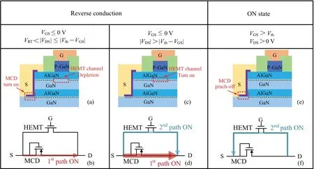
Fig.2.Current paths and equivalent circuits of the DCRC-HEMT at different operation states.
3.Results and discussion
Figure 3(a) gives the log-scale reverse conduction characteristics to clearly illustrateVRT.TheVRTis defined as the|VDS| at|IDS| = 1 mA/mm.For DCRC-HEMT, whenVRT<|VDS|≤|Vth-VGS|, only the 1stpath is turned on, as shown by pointM, which is only controlled by MCD instead ofVGS.Therefore, theVRTof DCRC-HEMT is independent ofVGS.WhenVGSvaries from 0 V to-1 V, theVRTof the DCRC-HEMT keeps 0.62 V(i.e.,at pointsMandM′),while theVRTof Conv.HEMT shifts from 1.54 V to 2.57 V,denoted as the green arrow fromOtoPpoint in Fig.3(a).Compared with the Conv.HEMT,the DCRC-HEMT realizes 59.7%and 75.9% reduction of theVRTatVGS=0 V and-1 V, respectively.For the curves of DCRC-HEMT,the current deviation between the solid and dashed lines at pointO′suggests the turn-on of the 2ndpath.The turn-on voltage of the 2ndpath(i.e., at pointO′) is equal to that of the Conv.HEMT, i.e., atVRT=1.54 V at pointO.Figure 3(b) shows the linear-scale reverse current through the 1stpath (|I1|) and 2ndpath (|I2|)in DCRC-HEMT atVGS=0 V and-1 V,which satisfies the equation|I1|+|I2|=|IDS|.It can be verified that the deviation of|IDS| and|I1| occurs at pointO′with 1.54 V or at pointP′with 2.57 V, which corresponds to the turn-on voltage of the 2ndpath atVGS=0 V or-1 V,respectively.Figures 3(c)–3(f)demonstrate the turn-on sequence of the 1stpath and 2ndpath and their corresponding turn-on voltages on the condition ofVGS=0 V and-1 V.
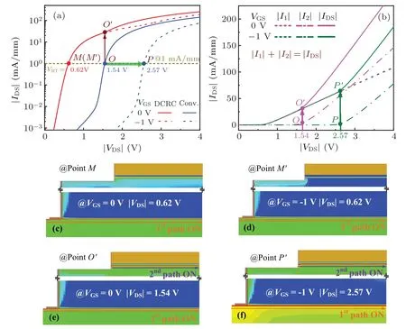
Fig.3.Reverse conduction characteristics of the devices: (a)log-scale coordinate and(b)linear-scale coordinate.(c)–(f)Current contours for DCRC-HEMT at different conditions.
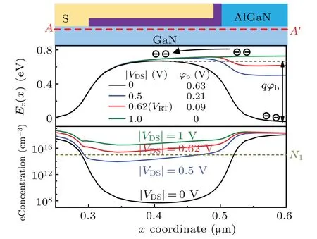
Fig.4.Conduction band energy extracted and electron concentration distribution along cutline AA′.
Figure 4 shows the extracted conduction band energy curves (Ec(x)) and electron concentration distributions along the cutlineAA′at different|VDS|,respectively.When|VDS|increases from 0 V to 0.62 V and 1 V, the barrier height (qφb)steadily decreases and even disappears.The HfO2/GaN interface under the source metal changes from depletion to accumulation state, and the electron concentration increases from lower thanN1to higher thanN1(although is still lower than the concentration of 2DEG).As a result, the MCD is turned on.
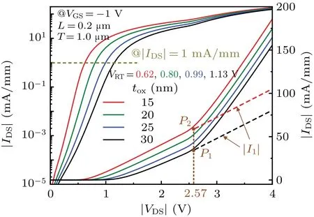
Fig.5.Reverse conduction characteristic as a function of tox.
Figure 5 shows the log-scale and linear-scale reverse conduction characteristics of DCRC-HEMT as a function oftoxatVGS=-1 V.The thickertoxleads to a weaker electron accumulation effect along the channel in MCD,therefore,theVRTincreases from 0.62 V at 15 nm to 1.13 V at 30 nm.However,the turn-on of the 2ndpath is independent oftox, so pointsP1andP2almost keep the same value of 2.57 V as discussed in Fig.3.
Figures 6(a) and 6(b) show the influence ofLon reverse conduction characteristics andBV.It can be seen in Fig.6(a)thatVRTincreases slightly with the increasingL.As shown in Fig.6(b),BVis sensitive to the variation ofLwhenL ≤0.15 μm.However, whenL ≥0.20 μm, theBVandVRTof MCD almost keep constant.The optimized region represented in Fig.6(b) could simultaneously fulfill the requirement of highBVand lowVRT.Figure 6(c) shows theEc(x)and electron concentration distributions along the cutlineAA′(see Fig.4)at differentL.Owing to the short-channel effect,both the barrier height and width decrease with the decreasingLwhenL <0.15 μm.Figures 6(d)–6(e)compare the leakage current distribution along MCD withL=0.1 μm and 0.2 μm at their ownBVs of 459 V and 686 V.As a result, the shortchannel effect in DCRC-HEMT withL=0.1 μm would lead to premature punch-through breakdown withIDS=1 μA/mm at the forward blocking state.
Figure 7 shows the blocking characteristics of the DCRCHEMT with differentT.High potential from drain is conducted through the 1stpath of low resistance, attracting electrons from the source.The lowerTmeans the lower distributed resistanceRfrom the source to the 1stpath.Therefore, more electrons are prone to flow through the 2ndGaN vertically to the 1stpath.Thus, to suppress the high leakage current,Tshould not be too low.
Figure 8 gives the transfer and output characteristics of DCRC-HEMT and Conv.HEMT.Figure 8(a) shows that the DCRC and Conv.HEMT exhibit normally-off operation withVth=1.52 V and 1.54 V atIDS=1 mA/mm,respectively.Figure 8(b) indicates that the on-state performances of DCRCHEMT almost keep consistent with that of the Conv.HEMT,which is because the 1stpath does not contribute to the forward conduction.
Figure 9 shows the key fabrication of the DCRC-HEMT,which starts with forming 110-nm-thick p-GaN on a doublechannel heterostructure based on the GaN-on-Si platform.The mesa isolation is fabricated by Cl2/BCl3-based inductively coupled plasma(ICP).Then the p-GaN gate is etched by ICP and passivation layers are formed by low pressure chemical vapor deposition (LPCVD) in Fig.9(b).Afterwards, digital etching is used to form the source and drain trenches and mitigate the damages, including ICP etching, plasma oxidation and wet-etching in Fig.9(c).Subsequently, dielectric deposition is carried out after the surface treatment, followed by partial etching to expose the source and drain Ohmic contact region, as shown in Fig.9(d).In Fig.9(e), a metal stack of Ti/Al/Ni/Au is deposited with the low-temperature Ohmic process and then is lifted-off to form the source/drain contact.Finally,the gate electrode is formed by e-beam evaporation and lift-off after selectively removing SiNxby reactive ion etching(RIE)in Fig.9(f).

Fig.7.(a) Forward blocking characteristics of DCRC-HEMT with different T (0.4–1.0 μm), and leakage current flowlines distributions of DCRC-HEMT at point(b)D,(c)E and(d)F.

Fig.8.(a)Transfer characteristic and(b)output characteristic of DCRC and Conv.HEMT.

Fig.9.Key fabrication of the DCRC-HEMT.(a)Epitaxy.(b)Gate definition and passivation layers formation.(c)Source/drain ohmic trench formation.(d)Source dielectric stack formation.(e)Source/drain electrodes.(f)Gate electrode.
4.Conclusion
In summary, a novel double-channel reverse conducting GaN HEMT with an integrated MOS-channel diode is proposed.The DCRC-HEMT provides an extra reverse current path to significantly improve the reverse current capability,maintaining the high on-state and blocking performances at the same time.TheVRTof 0.62 V of the DCRC-HEMT is not only low but also independent ofVGSandVth.As a result,the proposed DCRC-HEMT has the potential to reduce reverseconducting loss in power switching applications.
Acknowledgements
Project supported by the National Natural Science Foundations of China(Grant Nos.61874149 and U20A20208)and the Outstanding Youth Science and Technology Foundation of China(Grant No.2018-JCJQ-ZQ-060).

- Chinese Physics B的其它文章
- Robustness of community networks against cascading failures with heterogeneous redistribution strategies
- Identifying multiple influential spreaders in complex networks based on spectral graph theory
- Self-similarity of complex networks under centrality-based node removal strategy
- Percolation transitions in edge-coupled interdependent networks with directed dependency links
- Important edge identification in complex networks based on local and global features
- Free running period affected by network structures of suprachiasmatic nucleus neurons exposed to constant light