
High-temperature continuous-wave operation of 1310 nm InAs/GaAs quantum dot lasers
2023-10-11 07:56:28XiangBinSu蘇向斌FuHuiShao邵福會(huì)HuiMingHao郝慧明HanQingLiu劉汗青ShuLunLi李叔倫DeYanDai戴德炎XiangJunShang尚向軍TianFangWang王天放YuZhang張宇ChengAoYang楊成奧YingQiangXu徐應(yīng)強(qiáng)HaiQiaoNi倪海橋YingDing丁穎andZhiChuanNiu牛智川
Chinese Physics B 2023年9期
Xiang-Bin Su(蘇向斌), Fu-Hui Shao(邵福會(huì)), Hui-Ming Hao(郝慧明), Han-Qing Liu(劉汗青),Shu-Lun Li(李叔倫), De-Yan Dai(戴德炎), Xiang-Jun Shang(尚向軍), Tian-Fang Wang(王天放),Yu Zhang(張宇), Cheng-Ao Yang(楊成奧), Ying-Qiang Xu(徐應(yīng)強(qiáng)), Hai-Qiao Ni(倪海橋),Ying Ding(丁穎), and Zhi-Chuan Niu(牛智川),?
1State Key Laboratory for Superlattices and Microstructures,Institute of Semiconductors,Chinese Academy of Sciences,Beijing 100083,China
2Center of Materials Science and Optoelectronics Engineering,University of Chinese Academy of Sciences,Beijing 100049,China
3Beijing Academy of Quantum Information Sciences,Beijing 100193,China
4James Watt School of Engineering,University of Glasgow,Glasgow,G12 8LT,UK
Keywords: InAs/GaAs quantum dots,high-operating-temperature laser,molecular beam epitaxy(MBE)
1.Introduction
High temperature resistant semiconductor lasers have prospective applications in many situations, such as light sources for data transmission,[2]optical sensing and fiber gyros in a variety of harsh environments, even including applications for underground exploration of natural resources.Self-assembled quantum dots(QDs)of InAs/GaAs have raised great interest for the realization of high-performance laser diodes, owing to their low threshold current density, high quantum efficiency and stability at high temperature.[3–7]The semiconductor near-infrared laser diode market has been dominated by InP-based materials for a long time, but one of the limitations of InP-based lasers is that when working at elevated temperature, a thermoelectric cooler or a thermal dissipation platform is needed.For InAs/GaAs QD lasers, when the density of the QDs is further improved under the same multi-layered structure the optical gain can be sharpened and maximum gain is increased without changing the laser optical mode,thus increasing the characteristic temperature of the laser and resulting in a wider application field for QD lasers.
With much progress being made in molecular beam epitaxy(MBE)technology,the development of QD lasers has also greatly benefited.MBE is an epitaxial technology particularly suited for the preparation of advanced materials, heterostructures and nanostructures.Various investigations have been reported for optimizing the parameters to obtain high-quality QDs.Metal–organic chemical vapor deposition(MOCVD)is one of the typical deposition techniques employed.[8,9]However, it is difficult to fabricate As-based high-performance QD lasers using MOCVD.[10,11]MBE is a more suitable method,and the interruption growth mode of QDs,[12]growth temperature[13]and multistacking QD layers[14,15]are factors proposed to enhance the surface dot density.While these do improve the dot density to (4–5)×1010cm-2, introduction of single large QDs is also seen and this degrades the QD uniformity.[16,17]In order to enhance the QD quality further, suppression of the introduction of single large QDs needs to be achieved.Various methods, such as increasing the surface adatom mobility,[16]introducing a strain reducing layer(SRL)[18]and optimizing the growth rate,[19,20]have been investigated for improving QD size uniformity.A recent study by Liu’s group systematically improved the QD dot-height uniformity, obtaining a linewidth of 30 meV with a density of 4.5×1010cm-2and 42 meV with a density of 5.8×1010cm-2.[21]Thus far, few comprehensive investigations for improving both dot density and size uniformity have been done.We aim to further optimize the growth parameters to obtain high dot density and high size uniformity.
In this paper, we applied annealing during active region growth in the MBE chamber and successfully eliminated the bimodal size distribution in InAs/InAs QDs by optimizing annealing temperature and annealing layer position.[22,23]Based on that,by optimizing the deposition rate,growth temperature and As pressure of InAs,we improved the density of QDs and their monolayer uniformity, which increased optical gain in broad area lasers.In addition,we have prepared high-density(5.9×1010cm-2)InAs/GaAs QD lasers and also low-density(3.0×1010cm-2)QD lasers with the same active region stack for comparative experiments.
2.Material growth
The InAs/GaAs quantum dots were grown in a Veeco Gen 930 MBE system, and the epitaxial structure is shown in Fig.1.The growth began with deoxidation and oxide desorption was performed by holding the GaAs substrate at a temperature of 680°C for 10 min in the chamber.The substrate was then cooled down to 620°C for growing a 500 nm GaAs layer as the buffer layer and a 1800 nm ndoped Al0.45Ga0.55As layer as the cladding layer.The active region was grown between the top and bottom undoped waveguide layers;the thickness of both waveguide layers was 200 nm.Then a 1800 nm p-doped Al0.45Ga0.55As layer was deposited followed by a 200 nm p-doped GaAs layer on top of it for electrical contact.The doping density of the buffer layer,cladding layer and electrical contact layer was 2×1018cm-3,2×1018cm-3and 1×1019cm-3,respectively.
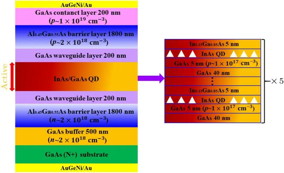
Fig.1.Schematics of the epitaxial structure of an InAs/GaAs QD laser.
The active region contained five sets of InAs/GaAs QDs and partially p-doped GaAs as the initial p-type modulation layer.Then the temperature of the substrate was reduced to 525°C for the growth of 2.1 monolayer(ML)InAs at a growth rate of 0.046 ML·s-1,followed by a 5-nm In0.15Ga0.85As layer to relieve the misfit stress[caused by the lattice constant mismatch between GaAs (5.65 ?A) and InAs (6.06 ?A)].The substrate temperature was kept at 540°C for the growth of 15 nm GaAs, and then up to 630°C and held for 5 min; this step can further eliminate dislocations and misfits within the interface.QD annealing could further eliminate the bimodal size in InAs/GaAs, and details of this are available in our previous report.[24]Then the temperature was reduced to 620°C for the growth of 25 nm GaAs.The reason why annealing was introduced after the 15 nm GaAs instead of the 5 nm In0.15Ga0.85As is that the desorption temperature of In is lower than that of Ga.If the annealing process immediately followed the In0.15Ga0.85As growth step, In would desorb and most of the misfit stress could not be released.The above experimental parameters were used to grow InAs/GaAs QDs at a density of 3.8×1010cm-2.The atomic force microscopy(AFM)test results are shown in Fig.2.
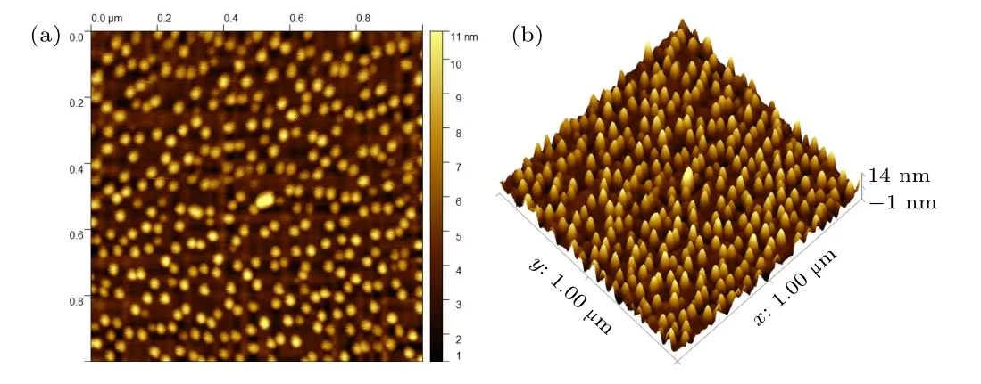
Fig.2.The 1 μm×1 μm AFM measurement of low-density QD testing sample.
On this basis,we continued to investigate a series of samples with varied growth parameters, namely, InAs deposition rate, deposition amount and growth temperature experiments to improve the QD density.The optimal experimental parameters for achieving a high density were obtained, the temperature of the substrate was set to 535°C for the growth of 2.45 ML InAs at a growth rate of 0.1 ML·s-1,and the cap layer structure and growth conditions are consistent with the former.With the above growth method,we obtained 5.9×1010cm-2ultra-high density InAs QDs.The AFM test results are shown in Fig.3 and the growth details including As pressure,growth temperature and shutter sequence are shown in Fig.4.

Fig.3.The 1 μm×1 μm AFM measurement of high-density QD testing sample.

Fig.4.Growth parameters for a period of InAs/GaAs QD growth:(a)shutter sequence,(b)temperature and As pressure.
3.Device fabrication and measurement result
A ridge waveguide laser with 100 μm ridge width and 2 mm cavity length was fabricated on the as-grown material.The ridge was fabricated using lithography and an inductively coupled plasma.The depth of the waveguide was 1.6 μm,with 200 μm SiO2grown on top of it by plasma enhanced chemical vapor deposition for isolation.After a 90-μm contact window had been fabricated on the top of the isolation layer, 50 nm Ti/50 nm Pt/1000 nm Au was deposited on top of it by magnetron sputtering as the p-type electrode.The backside process and other fabrication details have been reported in detail previously.[25]A cross-sectional schematic diagram and scanning electron microscope(SEM)image of the InAs/GaAs QD laser are shown in Fig.5.
The basic performance of two devices with different densities was tested.Both types of devices achieved continuous lasing at room temperature.The active region of the devices was low-density or high-density InAs/GaAs QDs.The device lasing spectrum andL–I–Vcurves for the low-density device are shown in Fig.6.The center wavelength of the lasing spectrum of both devices was 1300 nm and the maximum output power at room temperature for the low-density device was 650 mW.
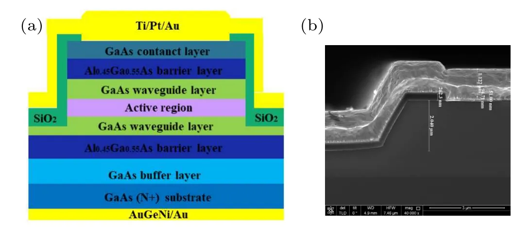
Fig.5.Schematic diagram and SEM image of a 1.3 μm InAs/GaAs QD laser.(a) Schematic diagram of a side view of the QD laser cavity.(b)SEM image of the side wall of the QD laser device;the height of the side wall is 2.04 μm.

Fig.6.(a)Power–current(P–I)characteristics and(b)spectrum for the low-density InAs/GaAs QD laser at room temperature.

Fig.7.(a) The P–I characteristics test of a high-density InAs/GaAs QD laser at temperatures between 5 °C and 110 °C.All continuous wave optical output power values presented in this graph are from a single facet.(b) Room temperature spectra of a 1.3 μm InAs/GaAs QD laser recorded for injection current densities between 0.25 kA·cm-2 and 1.00 kA·cm-2.Maximum intensities are normalized with respect to themselves for all measurements.
Compared with the low-density QD laser,a series ofP–Icharacteristic tests were conducted for the high-density InAs QD laser at temperatures between 5°C and 110°C with the assistance of a self-built temperature control thermoelectric cooler(TEC)module,as shown in Fig.7(a).In order to confirm that no device degradation occurs during the temperature measurement process, the temperature of 5°C was measured twice before and after this variable temperature test.The laser achieved considerable performance, the output power was as high as 131 mW at 110°C without visible degeneration and 1.030 W at room temperature with a threshold as low as 0.3 A.The laser spectral characteristics of the highdensity InAs/GaAs QD laser at room temperature are shown in Fig.7(b).The peak wavelength shifts from 1307.8 nm at a current density of 1.00 kA·cm-2to 1317.8 nm at 0.25 kA·cm-2.Once the injection current exceeds the threshold, increasing the current will not change the number of carriers in the active region.The number of electrons and holes is stable in the active region, which is different from the mechanism of wavelength shift below the threshold current.When injecting current above the threshold current,the temperature of the p–n junction increases with increasing injection current; consequently, the lasing wavelength shows a trend of a shift to a long wave band.Due to the advantage of three-dimensional quantum confinement effect in the QDs, the wavelength only shifts 10 nm when the injection current density quadruples from 0.25 kA·cm-2to 1.00 kA·cm-2.
4.Conclusion
Two kinds of InAs QDs with different densities in active regions were applied in a QD laser for emitting at 1.3 μm.The broad-area edge-emitting lasers were fabricated on the presented structure.In order to characterize the resulting high-density QD laser device,P–Itests were carried out in the temperature range between 5°C and 110°C.The roomtemperature spectra tests also showed that the wavelength of the QD lasers can be fixed at 1.3 μm over a broad injection current range.The output power is 131 mW at 110°C and 1.030 W at room temperature,with a threshold as low as 0.3 A.The performance of the high-density QD laser exceeds that of the low-density QD laser,because when the density of the QDs is further improved under the same uniformity and multi-layered structure the optical gain can be sharpened and maximum gain is increased without changing the laser optical mode, resulting in improving output power and characteristic temperature for QD lasers.
Acknowledgments
Project supported by the Science and Technology Program of Guangzhou (Grant No.202103030001), the Key-Area Research and Development Program of Guangdong Province (Grant No.2018B030329001), the National Natural Science Foundation of China (Grant Nos.62035017,61505196, and 62204238), the Scientific Instrument Developing Project of the Chinese Academy of Sciences(Grant No.YJKYYQ20170032), the Major Program of the National Natural Science Foundation of China (Grant Nos.61790580 and 61790581), the Chinese Academy of Sciences and Changchun City Science and Technology Innovation Cooperation Project (Grant No.21SH06),Jincheng Key Research and Development Project (Grant No.20210209), the Key R&D Program of Shanxi Province(Grant No.202102030201004), the R&D Program of Guangdong Province (Grant Nos.2018B030329001 and 2020B0303020001), Shenzhen Technology Research Project(Grant No.JSGG20201102145200001), and the National Key Technologies R&D Program of China (Grant No.2018YFA0306100).
- Chinese Physics B的其它文章
- Robustness of community networks against cascading failures with heterogeneous redistribution strategies
- Identifying multiple influential spreaders in complex networks based on spectral graph theory
- Self-similarity of complex networks under centrality-based node removal strategy
- Percolation transitions in edge-coupled interdependent networks with directed dependency links
- Important edge identification in complex networks based on local and global features
- Free running period affected by network structures of suprachiasmatic nucleus neurons exposed to constant light