Optimal Process Parameters of Preparing MoS2 Films by RF Magnetron Sputtering
2023-03-14 13:56:14,,,,,,
人工晶體學(xué)報 2023年2期
, , , , , ,
(School of Sciences, Henan University of Technology, Zhengzhou 450001, China)
Abstract:MoS2 films were prepared on quartz substrate by radio frequency (RF) magnetron sputtering. The effect of sputtering time, sputtering temperature, argon flow rate and sputtering power on the structure of MoS2 films was studied by orthogonal test method. The crystallinity, thickness and surface morphology of MoS2 films were analyzed by XRD, Raman, XPS, EDS and SEM, the optimal process parameters for preparing MoS2 films were obtained. It is found that the crystallinity of the sample is poor at higher or lower sputtering temperature, and the XRD diffraction peak of the sample is not obvious at lower sputtering temperature. When the temperature is 250 ℃, the sample has more XRD diffraction peaks and better crystallinity. According to the orthogonal test, sputtering temperature plays a crucial role in the crystallization of MoS2, followed by argon flow rate. When sputtering temperature is 250 ℃, argon flow rate is 6 mL/min, sputtering time is 30 min, and sputtering power is 300 W or 400 W, the crystallinity of MoS2 film is better. The film prepared under this condition is thicker, but it points out the direction for future experiments. In the following experiments, sputtering temperature, sputtering power and argon flow rate can be kept unchanged. By shortening the time, films with a thickness of 58.9 nm have been successfully prepared.
Key words:MoS2 films; RF magnetron sputtering; two-dimensional material; orthogonal test method; process parameter
0 Introduction
In recent years, two-dimensional (2D) materials, for instance, graphene and transition metal dichalcogenides (TMDCs) have attracted enormous research interests[1-4]. Molybdenum disulfide (MoS2), a unique transition-metal disulfide that is abundant in nature[5-7], is supposed to be a two-dimensional material because its thickness can be adjusted from bulk to monolayer[8-11]. MoS2has been broadly used in memory devices, sensors, optoelectronic devices, and biomedical fields due to its excellent physical and chemical properties[12-14]. The main techniques for preparing single-layer or few layer MoS2film materials are: micromechanical exfoliation, solution exfoliation, chemical vapor deposition (CVD)[15], wet chemical method, hydrothermal synthesis, and physical vapor deposition (PVD)[16]. However, the properties of MoS2prepared by different preparation method are significantly different. CVD method has the advantages of fast film forming speed and large area. Still, this method has defects such as high reaction temperature, environmental pollution by residues, and equipment corrosion. Due to the fast film forming speed, and uniform particle size, magnetron sputtering technology can be used to prepare MoS2films with various properties, so the method commonly used in industry[17]. But the crystal structure changes caused by magnetron sputtering process parameters are not clear and there are few literature reports. In terms of substrate, silicon substrates are used more than quartz substrates in most experiments[18]. MoS2films prepared with silicon substrates can be used as field effect transistor and heterojunction, while MoS2films prepared with quartz substrates can be used as photodetector. Therefore, further investigation of preparation technology and performance of MoS2films is indispensable.
In the literature reports, most of the MoS2films were prepared on silicon substrate by variable-controlling method[19]. However, it is difficult to get optimum process parameters using the variable-controlling method because of the complex preparation conditions. In this paper, optimum process parameters for preparing MoS2films from orthogonal tests were obtained and MoS2films on quartz substrates by radio frequency (RF) magnetron sputtering were successfully prepared.
1 Experimental section
1.1 Preparation of MoS2 films
MoS2films were deposited on quartz substrates by RF magnetron sputtering, argon (Ar, purity 99.99%) was selected as sputtering gas. High-purity MoS2(MoS2, purity 99.99%) was selected as the target material. Quartz substrates were cleaned with absolute ethanol and deionized water. The working pressure is 1.0×10⁻³Pa. It is found that sputtering time, substrate temperature, argon flow rate, and sputtering power have a significant influence on the experimental results, so these four factors are selected as experimental conditions. Table 1 is the factor level table of the orthogonal experiment design. Sixteen samples were prepared for the experiment. Four factors (A, B, C, and D) represent sputtering time, sputtering temperature, argon flow rate, and sputtering power, respectively. The orthogonal test scheme was obtained in Table 2[20].

Table 1 Orthogonal test table with 4 factors and 4 levels
Table 2 Orthogonal test table of 16 samples combined by 4 factors and 4 levels
1.2 Characterization of MoS2 films
The microstructures of the deposited films were characterized by 8D Discover X-ray diffraction (XRD) analysis and Renishaw inVia Raman at an excitation light of 532 nm. The chemical composition and bonding of the films were characterized by Multifunctional X-ray photoelectron spectroscope (XPS; Axis ultra dld, Japan). The thickness and morphology of the films were determined by scanning electron microscopy (SEM; S-4800, Hitachi, Tokyo, Japan). The elemental composition and atomic percentage of the films were measured using an X-ray energy spectrometer (EDS; S-4800, Hitachi, Tokyo, Japan).
2 Results and discussion
2.1 XRD patterns
Fig.1 displays different diffraction peaks of 16 samples. The ICSD indicates that the diffraction peaks are 13.5°, 28.1°, 31.9°, 33.5°, and 59.0° correspond to (002), (021), (100), (101), and (110) crystal planes of MoS2. Sharp diffraction peaks indicate prominent MoS2crystals on the surface of the quartz substrate[21]. In Fig.1(a), the 0# is the spectrum of a quartz substrate. All samples have the (101) crystal plane diffraction peak except for samples 1# and 14#, which means that most samples grow preferentially on the (101) crystal plane, followed by (100) crystal plane. In Fig.1(d), samples 15# and 16# have high diffraction peaks at 33.5°.
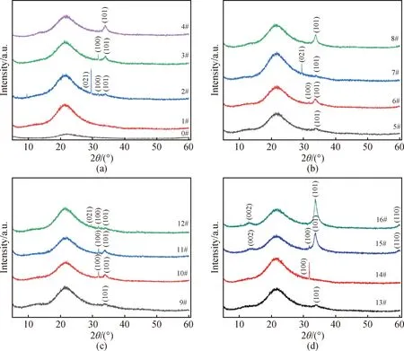
Fig. 1 XRD patterns of quartz substrate and sixteen samples
2.2 Raman spectra

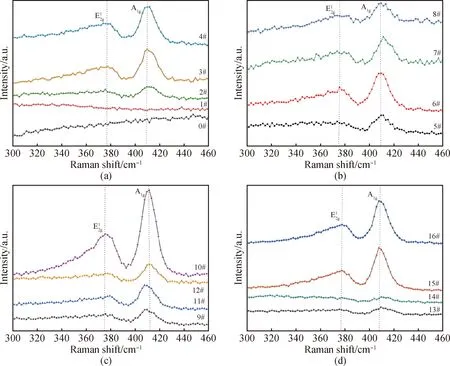
Fig.2 Raman spectra of quartz substrate and sixteen samples at an excitation light of 532 nm

Fig.3 Data analysis diagram of Raman and XRD
2.3 Effect of process parameters on the structure of MoS2 film
The height and width of XRD peak represent the grain size and crystallinity. The narrower and higher the peak, the larger the grain size, the more perfect the crystallization. On the contrary, the wider and lower the peak, the smaller the grain size, poor crystallization results in relatively small grains. The more the number of diffraction peaks, the better the crystallinity. To study the effect of process parameters on the structure of MoS2films, Table 3 gives the relationship between orthogonal design parameters and the number of XRD peaks. Taking the number of XRD diffraction peaks as the investigation index to investigate the effect of process parameters on the structure of MoS2film, as shown in Table 4.

Table 3 Relationship between orthogonal design parameters and the number of XRD peaks
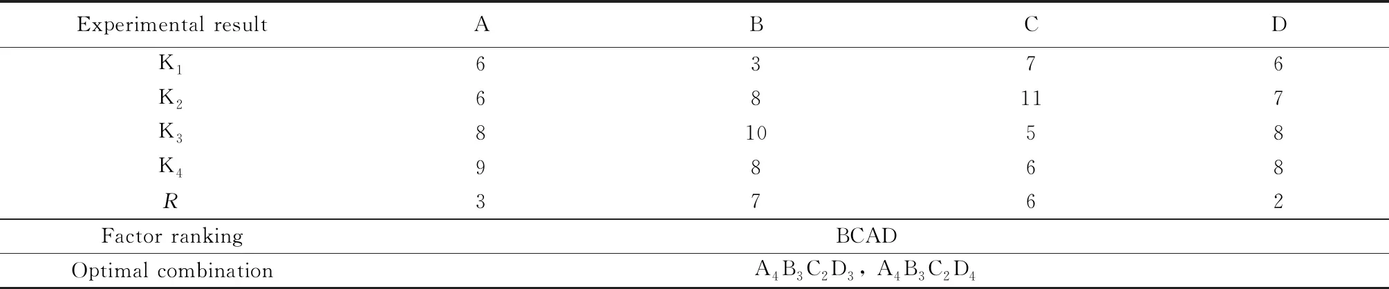
Table 4 Effect of process parameters on the structure of MoS2 film
In Table 4, it is shown that sputtering temperature plays the essential role in the crystallization effect of MoS2, followed by argon flow rate. And the best combination is A4B3C2D3, or A4B3C2D4(15#),i.e., sputtering temperature is 250 ℃, argon gas flow rate is 6 mL/min, sputtering time is 30 min, and sputtering power is 300 W or 400 W.
As shown in Table 2 and Table 3, when sputtering temperature is 250 ℃, the crystallinity of samples 3#, 7#, and 11# is relatively good and has two diffraction peaks. There are four diffraction peaks in the spectrum of sample 15# with optimally process parameters. When sputtering temperature is very low, samples 1#, 5#, 9#, and 13# have only one diffraction peak and the intensity is very low. It shows that the lower sputtering temperature is not good for the growth of MoS2films.
Although sputtering temperature of sample 4# has reached the maximum value, only the (101) crystal plane is crystallized due to the reduction of the mean free path of ions bombarding the substrate caused by the higher argon flow rate, which influences the etching of the film surface and film crystallization. So, argon flow rate is another indispensable influencing factor. When argon flow rate is too large, the number of diffraction peaks of XRD is minimal.
The third influence is factor sputtering time, which influence the number of layers of MoS2. When sputtering time increases, number of layers increases, which results in the appearance of the (002) and (110) crystal planes of sample 15# and 16#, as shown in Fig.1. It can be seen from the samples 1#, 7#, 12# and 14# that it is not conducive to the growth of the (101) crystal plane when the sputtering power is lower.
2.4 XPS
Through the above analysis, samples 1# and 5# with poor crystallization and samples 10# and 16# with better crystallization were selected for further characterization and analysis. Fig.4(a) exhibits the XPS, which verifies the existence of S and Mo elements[26]. As shown in the figure, 531.3eV corresponds to the XPS peak of O 1s and is attributed to the oxidation of the samples before testing. The C 1s peak at 283.8 eV is associated with adventitious carbon in XPS test. The peak positions of S 2p and Mo 3d of sample 1# are shifted relative to other samples. It suggests that there are Mo and S atoms in sample 1# but no MoS2crystals, which is consistent with the results of XRD.
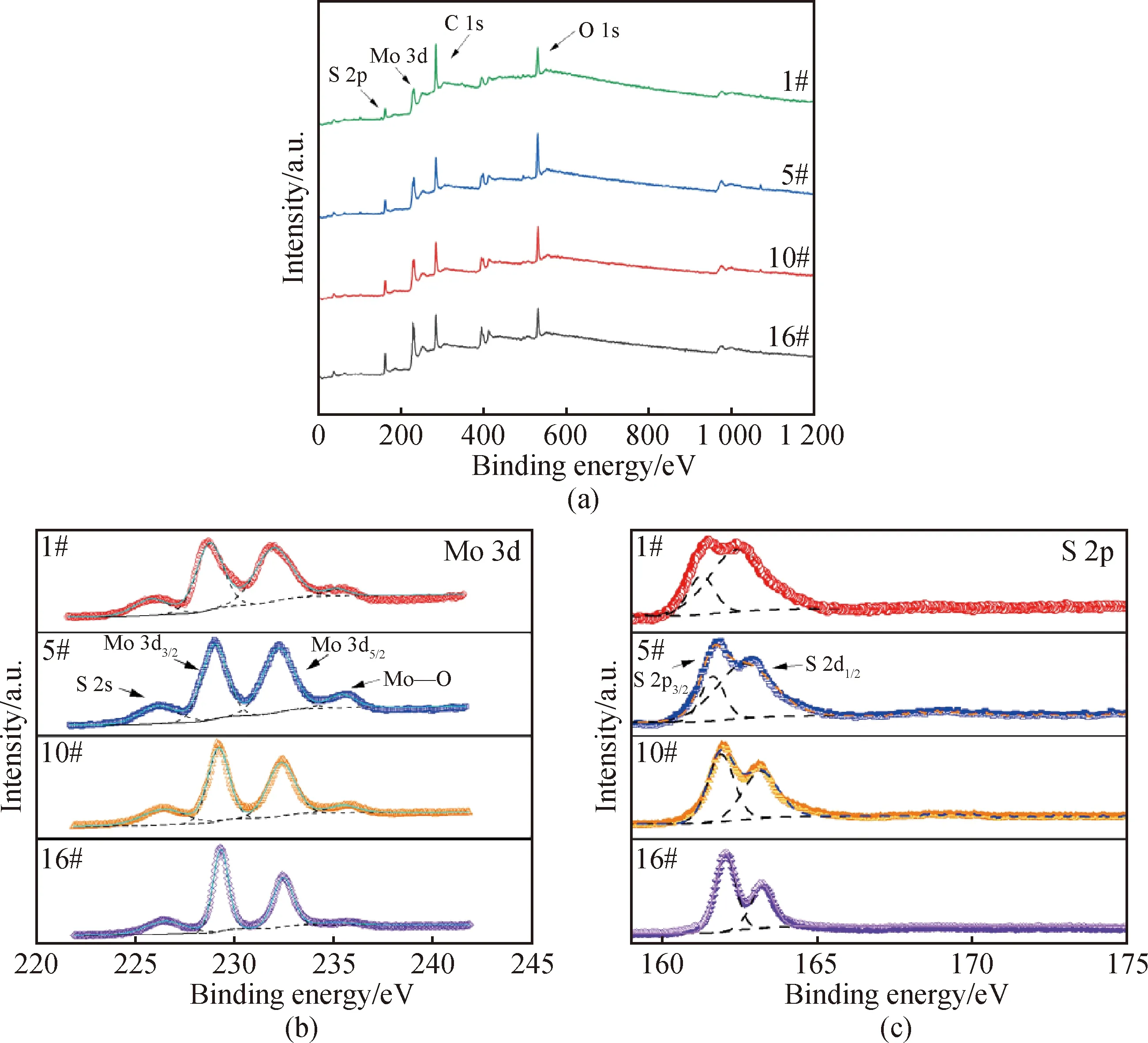
Fig.4 XPS spectra of four samples: (a) survey scan; (b) Mo 3d elemental scan; (c) S 2p elemental scan
Fig. 4(b) shows four peaks appearing at 226.5, 229.3, 232.4, and 235.1 eV in the Mo 3d spectrum[27]; these peaks correspond to S 2s, MoS2, and MoO3, respectively[28]. It can be seen that Mo 3d exhibits two spin-orbit characteristic peaks split into 3.10 eV. The high-intensity peaks of Mo 3d3/2at 229.3 eV and Mo 3d5/2at 232.4 eV are consistent with the literature[4,29]. Mo 3d3/2is typical of Mo4+in the MoS2lattice[30]. Furthermore, the peak at 235.1 eV identifies with the Mo—O bond[31], which demonstrates that the film surface is partly oxidized, and the S 2s peak occurs at 226.5 eV, indicating the formation of sulfide.
Fig.4(c) indicates the two spin-orbit characteristic peaks of the S 2p spectrum at 163.2 eV (S 2p1/2), and 162 eV (S 2p3/2) split into 1.16 eV are consistent with the literature[24,29], reflecting the S2-state in the MoS2lattice. It can be seen from the Fig.4 that sample 16# has a high peak strength, which is due to its good crystallization effect, that is consistent with XRD and Raman results.
2.5 EDS
Fig.5 gives the EDS and atomic percentage of the samples 5#, 10#, 15#, and 16#. Table 5 details the atomic percentages of the four elements in four samples. The EDS information indicates that the ratio of Mo to S atoms in samples 15# and 16# is approximately 1∶2[32]. This phenomenon indicates that MoS2exists in the films (and a small number of defects is also present)[33], which is identified with the results of XRD. It shows that with the increase in sputtering temperature and sputtering time, the crystallization of MoS2film is better. Moreover, EDS found the existence of O and Si atoms, the presence of O element is due to the oxidation of the sample before testing, and the presence of Si element is due to the quartz substrates.
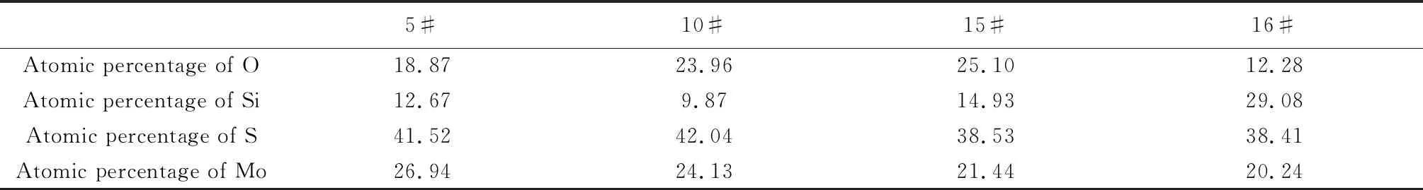
Table 5 Atomic percentages of O, Si, S, and Mo for four samples /%
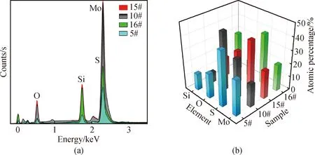
Fig.5 EDS (a) and atomic percentage (b) of the samples 5#, 10#, 15# and 16#
2.6 SEM
SEM image of samples 5#, 10#, 15#, and 16# are given in Fig. 6. It is observed that the four samples have dense surfaces and the particle size of the last three samples is uniform, but their process parameters are different[34]. Temperature is the most important factor affecting MoS2crystallization, followed by argon flow rate. Fig. 6 shows that the MoS2film prepared at the sputtering temperature of 200 ℃ is thicker. This result is consistent with the Raman test. Although the sputtering time of samples 15# and 16# is longer than that of sample 10#, their thickness is thinner than that of sample 10#. This is because sample 15# has the most suitable temperature and sample 16# has a low argon flow. Fig. 6 (c) shows the optimal process parameters of sample 15#.
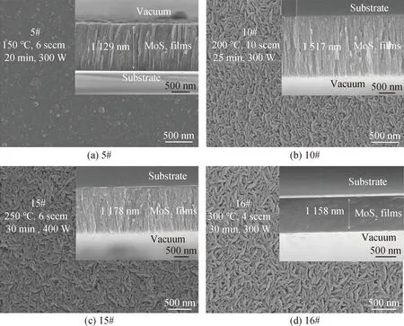
Fig.6 SEM images and cross-section images of samples
16 samples were prepared by magnetron sputtering, and it can be confirmed that temperature and argon flow rate have great influence. However, the prepared samples are all micron films instead of 2D materials. Next, by keeping sputtering temperature, argon flow rate and sputtering power constant and shortening sputtering time, thinner films can be prepared. Sample 17# with less time was prepared. The optimized process parameters were used for sample 17, but time was reduced, i.e.. The sputtering temperature, argon flow rate, and sputtering power were set to 250 ℃, 6 mL/min, and 300 W, respectively, sputtering time was reduced from 30 min to 1 min. Fig.7 shows the morphology and cross-section images of sample 17#. It can be seen from Fig. 7 that the surface of 17# sample is dense and thickness is 58.9 nm. It shows that the result of orthogonal test is feasible.
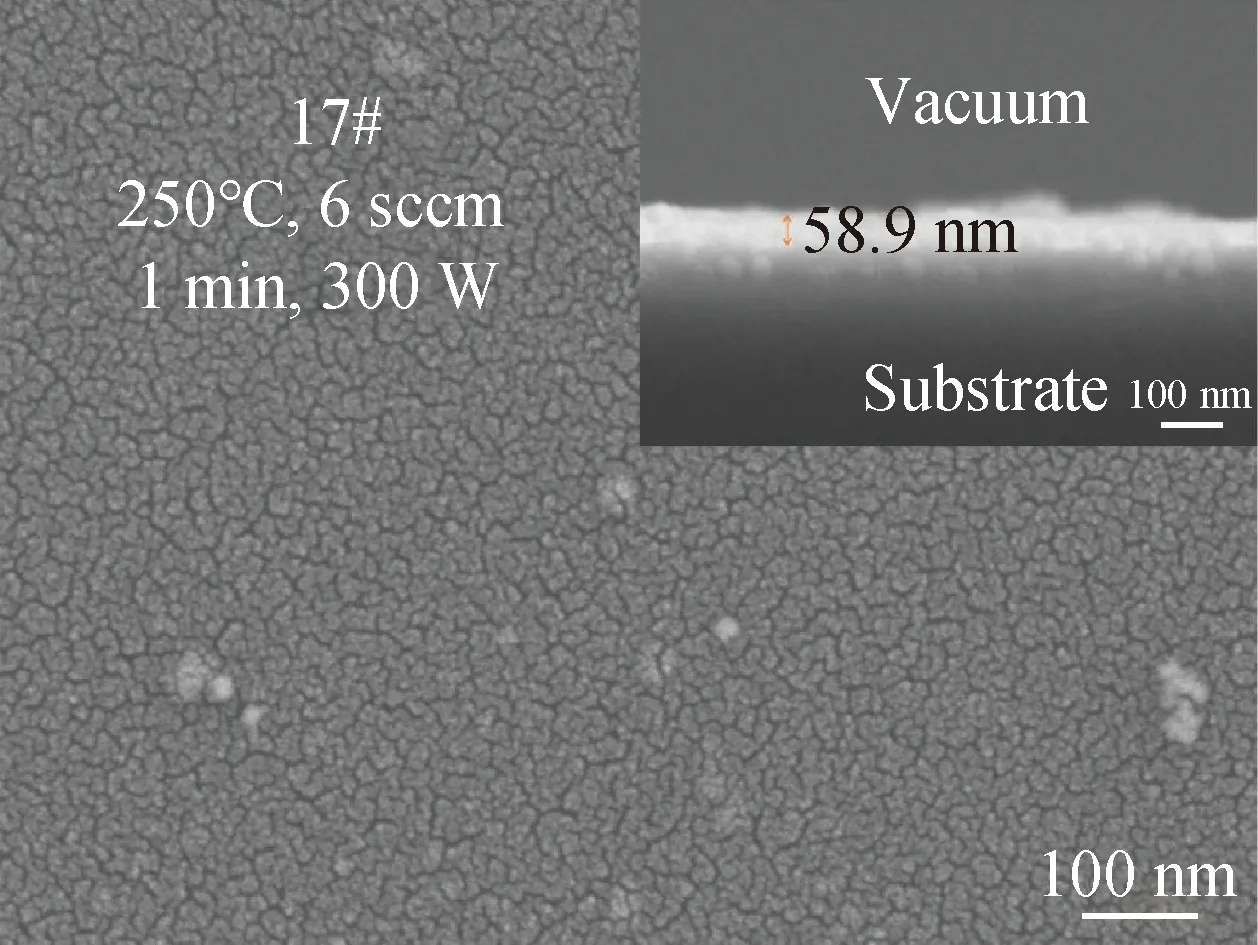
Fig.7 SEM image and cross-section image of samples 17#
3 Conclusion
MoS2films were prepared on quartz substrates by RF magnetron sputtering. The sputtering temperature plays an essential role in the crystallization effect of MoS2, followed by argon flow rate. Prepared MoS2films are in better crystallization when sputtering temperature is 250 ℃, argon flow rate is 6 mL/min, sputtering time is 30 min, and sputtering power is 300 or 400 W. As can be seen from XRD, MoS2film grows preferentially at (101) orientation, followed by the (100) crystal plane. XPS tests show that there are typical Mo4+in the prepared films, which prove the existence of MoS2. It can be seen from SEM with the increase in sputtering time, the thickest MoS2films were prepared under 200 ℃. The film prepared under orthogonal test conditions is thicker, by keeping the sputtering temperature, argon flow rate and sputtering power constant and shortening the sputtering time, 2D films were prepared.