
High-performance amorphous In–Ga–Zn–O thin-film transistor nonvolatile memory with a novel p-SnO/n-SnO2 heterojunction charge trapping stack
2023-02-20 13:16:40WenXiong熊文JingYongHuo霍景永XiaoHanWu吳小晗WenJunLiu劉文軍DavidWeiZhang張衛(wèi)andShiJinDing丁士進
Chinese Physics B 2023年1期
關鍵詞:張衛(wèi)
Wen Xiong(熊文), Jing-Yong Huo(霍景永), Xiao-Han Wu(吳小晗), Wen-Jun Liu(劉文軍),?,David Wei Zhang(張衛(wèi)),2, and Shi-Jin Ding(丁士進),2,?
1State Key Laboratory of ASIC and System,School of Microelectronics,Fudan University,Shanghai 200433,China
2National Integrated Circuit Innovation Center,Shanghai 201203,China
Keywords: nonvolatile memory,a-IGZO thin-film transistor(TFT),charge trapping stack,p-SnO/n-SnO2 het
1. Introduction
Amorphous indium gallium zinc oxide (a-IGZO)channel-based thin-film transistor(TFT)memory devices have been studied for flexible and transparent electronic devices and system-on-panel displays.[1,2]This can be attributed to several particular advantages of a-IGZO over conventional amorphous or polycrystalline silicon, including high-enough e-mobility, good electrical uniformity and high transparency to visible light.[3,4]Moreover, a-IGZO exhibits robust potential for back-end-of-line (BEOL) compatible memory for monolithic 3D integration because of a low thermal budget,integratable materials and processes, etc. However, since a-IGZO is intrinsically an n-type oxide semiconductor, it is difficult to produce hole conduction for a-IGZO channel transistors at negative gate biases. Therefore, the TFT memory device with an a-IGZO channel cannot be erased directly by injecting holes from the channel into its charge trapping layer(CTL), and it can only be erased by detrapping of electrons from the CTL. This usually results in rather low erase efficiencies for most a-IGZO TFT memory devices using metal nanocrystals or defects-rich dielectrics as a CTL due to high potential barriers for electron detrapping.[5–10]To achieve fast erasing behavior of the a-IGZO TFT memories, oxide semiconductor-based CTLs, such as sputtered a-IGZO[11–13]and atomic-layer-deposited ZnO,[14–16]have been explored in recent years. However, these a-IGZO TFT memory devices usually suffer from a trade-off between program/erase (P/E)efficiency and data retention.[17]For example, ZnO CTLbased memory devices exhibit distinct retention degradation;the ON/OFF readout current ratio decreases from 106to~103after 105s,[15]and even from~108to 1.8×10³after 104s.[16]Thus, how to obtain good data retention without sacrificing P/E efficiency is an urgent problem in existing memory technology.
In this work,a novel a-IGZO TFT memory is successfully demonstrated using a p-SnO/n-SnO2heterojunction charge trapping stack (CTS), and particularly exhibits both superior electrical P/E efficiency and good data retention. The underlying physical mechanism is also proposed based on the built-in electric field of the p–n heterojunction.
2. Experimental details
A p-type Si(100)wafer(ρ ≤0.005 Ω·cm)was used as the starting substrate, which served as the bottom gate of the fabricated devices. Then, a 35-nm Al2O3film was grown by atomic layer deposition (ALD) at 200°C as a blocking layer(BL). Then, a CTS of n-SnO2/p-SnO was deposited by reactive sputtering by changing the O2partial pressure (O2/Ar),followed by post-annealing in air at 250°C for 30 min. To obtain n-SnO2and p-SnO films, the O2partial pressure was kept at 40%and 12.9%,respectively,during sputtering.Meanwhile, the power and working pressure were maintained at 30 W and 2.6×10⁻³mbar,respectively. Thus,low deposition rates(2–2.9 nm/min)were obtained for the n-SnO2and p-SnO films; this could reduce sputter damage to the substrate surface.Subsequently,the CTS was defined by photo-lithography and wet etching,and then covered by a 10 nm ALD Al2O3film acting as a tunneling layer(TL).Next,a~40 nm a-IGZO film was deposited by magnetron sputtering at room temperature.The device channels were prepared by photolithography and wet etching. Source and drain contacts of Cr/Au were formed by sputtering and a lift-off technique. Finally, the fabricated device was annealed at 280°C in O2for 15 s.
The electrical characteristics of the a-IGZO TFT memory with a channel length/width (L/W=10/100 μm) were measured on a semiconductor device analyzer (Agilent B1500A)at room temperature in a dark box. The threshold voltage(Vth)was extracted as the gate voltage at which the drain current equaled toW/L×10-9A.
3. Results and discussion
Figure 1(a) shows a schematic diagram of the a-IGZO TFT memory with a heterojunction CTS,and a typical crosssectional TEM image of the fabricated memory is shown in Fig.1(b),clearly indicating the architecture of a-IGZO/Al2O3TL/n-SnO2/p-SnO/Al2O3BL.Figure 1(c)indicates that the n-SnO2and p-SnO films have optical direct bandgaps (Eg) of~3.31 eV and~2.45 eV,respectively,which are determined by plotting(αhυ)2versushυ. Furthermore,the XPS valence band spectra in Fig.1(d)also reveal different valence band onsets of the SnO and SnO2films, which are equal to 0.89 eV and 2.49 eV,respectively. This further confirms the formation of p-type SnO and n-type SnO2films.[18]
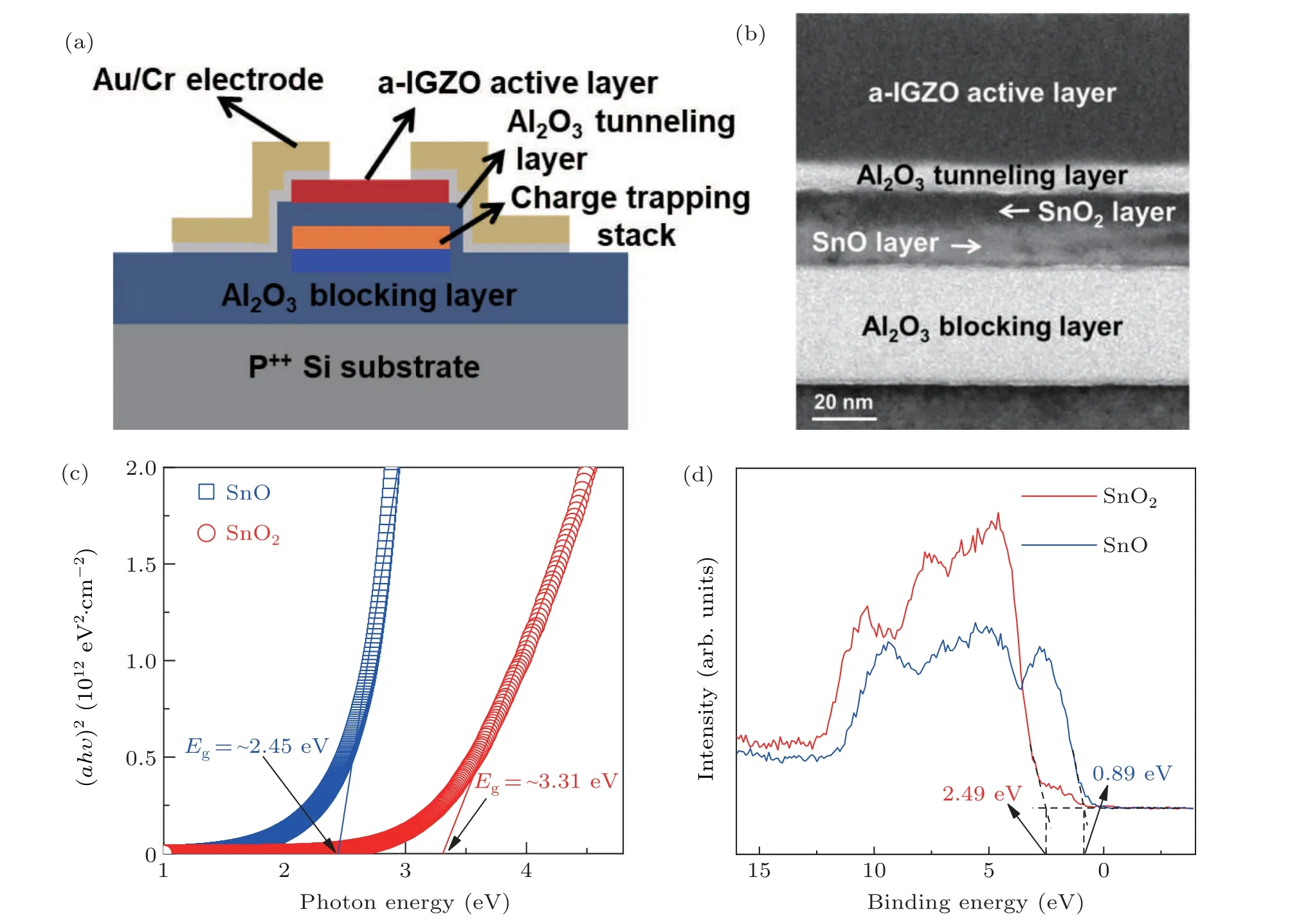
Fig.1. (a)A schematic diagram and(b)cross-sectional TEM image of the a-IGZO TFT memory with the n-SnO2/p-SnO CTS;(c)a plot of(αhυ)2 versus hυ to determine the direct optical bandgaps of the p-SnO and n-SnO2 films;(d)XPS valence band spectra of the p-SnO and n-SnO2 films.
Figures 2(a)and 2(b)show the P/E transfer characteristics of the a-IGZO TFT memory devices with single n-SnO2and p-SnO CTLs, respectively. With regard to the n-SnO2CTL,a positive threshold voltage shift(ΔVth)of 1.38 V is observed after programming at 14 V for 1 ms.However,after applying a gate bias of-8 V to the programmed device for 50 μs and even 1 ms,no ΔVthcan be distinguished.This indicates that the programmed device cannot be erased,which could be ascribed to the fact that n-SnO2has deep level defects(i.e.,~2.66 eV below its conduction band minimum),[19]thus the trapped electrons cannot be released back to the channel. In contrast, the p-SnO CTL gives rise to programmable and erasable characteristics,i.e.,ΔVth=2.28 V@14 V/1 ms,and ΔVth=-2.67 V@-8 V/50 μs. This is attributed to shallow defects in p-SnO.[20]However,this also causes the trapped electrons to be easily lost,resulting in poor data retention. As indicated in the inset of Fig.2(b),the p-SnO CTL device exhibits a charge loss rate of~97%at a retention time of 104s. As a comparison,after programming at 14 V for 1 ms, the n-SnO2CTL device only exhibits a charge loss rate of~2.7%,even at the retention time of 105s,as shown in the inset of Fig.2(a).
To obtain good data retention without sacrificing P/E efficiency, two CTSs composed of p-SnO and n-SnO2are further investigated while keeping the total thickness at 24 nm.Figures 3(a) and 3(b) show the P/E characteristics of the a-IGZO TFT memory devices with the n-SnO2/p-SnO and p-SnO/n-SnO2CTSs,respectively. In contrast to the unerasable characteristics of the single n-SnO2CTL device, both CTS memory devices exhibit considerable erase windows, i.e.,ΔVth=-4.82 V for the TL/n-SnO2/p-SnO/BL architecture,and ΔVth=-3.61 V for the TL/p-SnO/n-SnO2/BL architecture after erasing at-8 V for 50 μs. Further,figure 3(c)compares the cumulative program characteristics of the above two kinds of memory devices as a function of program bias and time, respectively. It is found that the architecture of TL/p-SnO/n-SnO2/BL gives rise to a larger program window than that of TL/n-SnO2/p-SnO/BL at a cumulative program voltage of≥12 V or cumulative program time of≥0.1 ms. Moreover,both exhibit comparable erase windows as a function of the cumulative erase voltage or time,as shown in Fig.3(d).
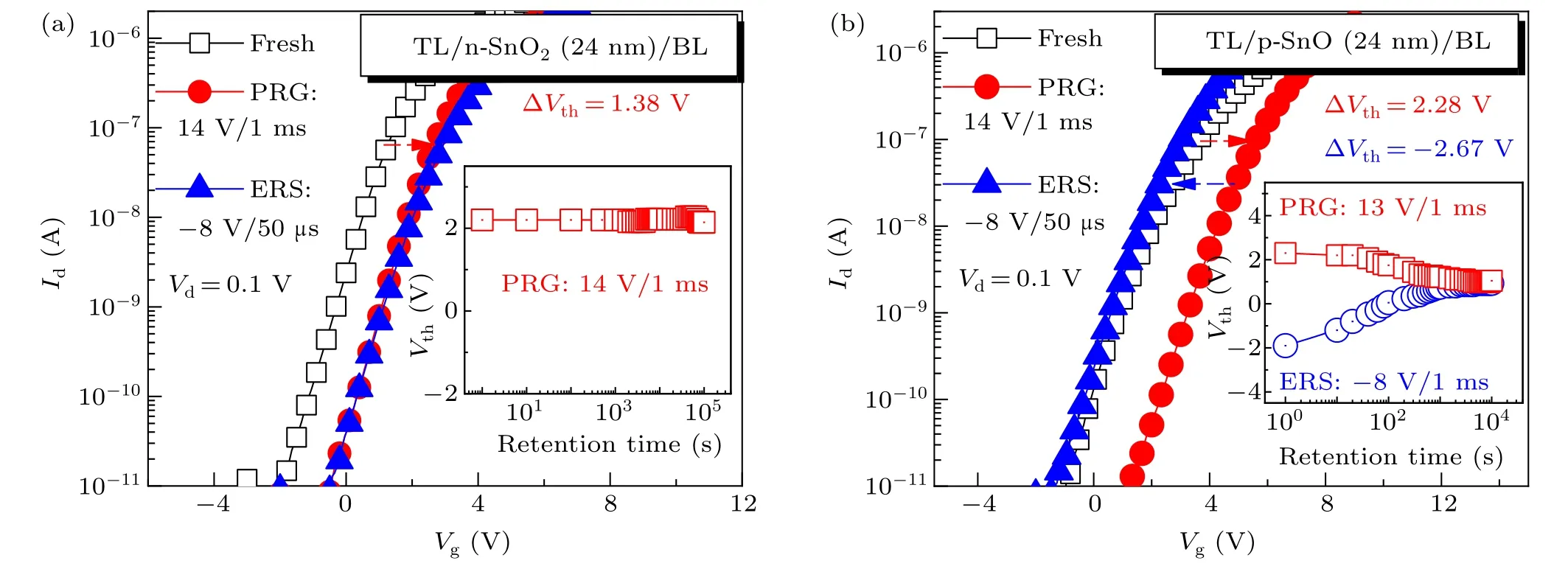
Fig.2. Transfer curves of the a-IGZO TFT memory devices with single n-SnO2 (a) and p-SnO (b) CTLs under fresh, programming (PRG) and erasing(ERS) modes, respectively. The inset in (a) shows the charge retention characteristic of the n-SnO2 CTL device, and the inset in (b) shows the retention characteristics of the p-SnO CTL device,revealing poor data retention.
Figure 4(a) shows the retention characteristics of the a-IGZO TFT memories with different architectures. It is indicated that the TL/p-SnO/n-SnO2/BL architecture demonstrates better data retention and a larger memory window(MW) than the TL/n-SnO2/p-SnO/BL architecture. For instance,the former shows a degeneration rate of~15%at the retention time of 105s,which is much smaller than~34%for the latter. Further, ten-year MWs are extrapolated, which are equal to 4.41 V and 3.24 V for the TL/p-SnO/n-SnO2/BL and TL/n-SnO2/p-SnO/BL architectures,respectively.
Table 1 summarizes the performance of the reported a-IGZO TFT memories in comparison with this work. Our memory with the TL/p-SnO/n-SnO2/BL architecture exhibits the largest initial MW, even under a much lower erase bias(-8 V),as well as the largest remaining MW of 5.62 V at the retention time of 105s. Compared with Refs. [7,20], our device demonstrates a rise of 6%–9%in charge loss,but the P/E speed increases around 10 and 100 times,respectively. Therefore,from the viewpoint of overall performance,our memory outperforms other reports. Moreover, such a large memory window can also compromise the negative effect incurred by relatively high charge loss.
To clearly understand the underlying mechanism, we measured the valence band maximum spectra and XPS corelevel spectra(Sn 3d5/2,Al 2p,O 1s)of the Al2O3,n-SnO2and p-SnO films(not shown here), and then the valence and conduction band offsets (VBO and CBO) were calculated, i.e.,VBO=0.63 eV and CBO=3 eV for the Al2O3/n-SnO2interface, and VBO = 3.05 eV and CBO = 1.44 eV for the Al2O3/p-SnO interface. Under these conditions, schematic band diagrams of the memory devices with n-SnO2/p-SnO CTSs are illustrated in Fig.4(b). It is well known that a builtin electric field (Ebuilt-in) can be generated at the interface of the p–n heterojunction. During programming under a positive gate bias, theEbuilt-in for the TL/p-SnO/n-SnO2/BL architecture has the same direction as that of the applied electric field(Eapplied), so the electric field across the heterojunction is enhanced. This accelerates the injected electrons moving from shallow traps in p-SnO to deep traps in n-SnO2,thus leading to a higher program efficiency,as demonstrated in Fig.3. During erasing under a negative gate bias,detrapping of the electrons captured in the shallow levels of the p-SnO layer dominates the erase window. This is because the electrons trapped in the n-SnO2layer find it hard to escape from the deep levels,especially under a reduced electric field across the heterojunction.This is why comparable erase characteristics are demonstrated for both CTSs. Furthermore, since most electrons are stored in the deep levels of the n-SnO2film after programming, the TL/p-SnO/n-SnO2/BL architecture can achieve excellent data retention.

Table 1. Comparisons of the P/E and data retention characteristics of the reported a-IGZO TFT memories and our devices.

Fig.3. Transfer curves of the a-IGZO TFT memory devices with (a) TL/n-SnO2/p-SnO/BL and (b) TL/p-SnO/n-SnO2/BL architectures under fresh, PRG and ERS modes,respectively. The comparisons of the cumulative(c)program and(d)erase characteristics as a function of P/E bias and time,respectively,for the above memory devices.
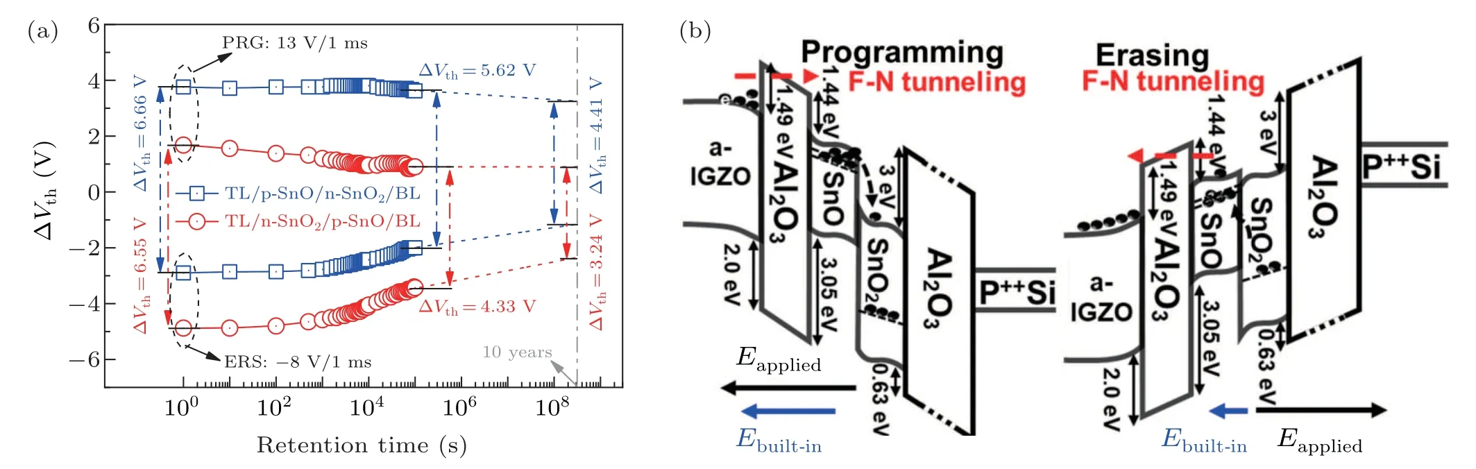
Fig.4. (a)The retention characteristics of the a-IGZO TFT memories with different architectures. (b)Schematic energy band diagrams for the TL/p-SnO/n-SnO2/BL architecture under programming and erasing modes,respectively.
4. Conclusion
In summary, compared to a single p-SnO or n-SnO2charge trapping layer, high performance a-IGZO TFT memories are achieved using novel p-SnO/n-SnO2heterojunction CTSs. High program and erase efficiencies as well as robust data retention are demonstrated,especially for the TL/p-SnO/n-SnO2/BL architecture. Finally, the underlying mechanisms are discussed. This work provides new insights into building a high program/erase efficiency,low power consumption, BEOL-compatible TFT memory based on oxide semiconductors.
Acknowledgment
Project supported by the National Natural Science Foundation of China(Grant No.61874029).
猜你喜歡
三角洲(2024年15期)2024-12-31 00:00:00
三角洲(2024年15期)2024-12-31 00:00:00
三角洲(2024年15期)2024-12-31 00:00:00
藝術學研究(2022年6期)2023-01-16 05:48:04
散文詩(2022年10期)2022-06-01 02:41:04
散文詩(青年版)(2022年5期)2022-05-31 01:42:12
散文詩(青年版)(2022年5期)2022-05-31 01:42:12
畫刊(2018年4期)2018-04-24 12:14:33
畫刊(2016年4期)2016-11-01 21:34:18
畫刊(2016年3期)2016-11-01 21:33:41
- Chinese Physics B的其它文章
- LAMOST medium-resolution spectroscopic survey of binarity and exotic star(LAMOST-MRS-B):Observation strategy and target selection
- Vertex centrality of complex networks based on joint nonnegative matrix factorization and graph embedding
- A novel lattice model integrating the cooperative deviation of density and optimal flux under V2X environment
- Effect of a static pedestrian as an exit obstacle on evacuation
- Chiral lateral optical force near plasmonic ring induced by Laguerre–Gaussian beam
- Adsorption dynamics of double-stranded DNA on a graphene oxide surface with both large unoxidized and oxidized regions