
Band alignment in SiC-based one-dimensional van der Waals homojunctions?
2021-12-22 06:49:22XingYiTan譚興毅LinJieDing丁林杰andDaHuaRen任達(dá)華
Chinese Physics B 2021年12期
Xing-Yi Tan(譚興毅) Lin-Jie Ding(丁林杰) and Da-Hua Ren(任達(dá)華)
1Department of Physics,Chongqing Three Gorges University,Wanzhou 404100,China
2School of Information Engineering,Hubei Minzu University,Enshi 445000,China
Keywords: SiCNTs/SiCNRs one-dimensional (1D) van der Waals homojunctions (vdWh), electronic structure,external electric field,axial strain
1. Introduction
Since graphene was successfully discovered, lowdimensional materials have attracted more and more attention due to their potential applications in electronic and spin devices.[1–4]Various efforts have been made to investigate the low-dimensional materials with a natural bandgap, such as phosphorene,[5,6]MoS2,[7–9]and monolayer GaN.[10,11]Recently,several low-dimensional SiC structures,including zerodimensional (0D) nanoparticles and nanospheres, and onedimensional (1D) SiC nanotubes (SiCNTs) and nanowires,have been constructed and promoted various researches in this area.[12–17]For instance, it was discovered that single wall SiCNTs are stable and have the characteristics of helicityindependent semiconductors.[18–22]Meanwhile, the theoretical prediction for stability of graphene-like SiC monolayers encouraged researchers to study the SiC nanosheets and nanoribbons(SiCNRs).[23,24]It was discovered that the behaviors of SiC nanosheets and armchair SiCNRs are favourite to non-magnetic (NM) wide bandgap semiconductors, whereas zigzag SiCNRs are magnetic and have metallic or halfmetallic features in the presence of narrow width.[25]According to these researches,low-dimensional SiC materials are potential candidates in nano-electronic and spintronic devices.
On the other hand, since the van der Waals heterostructures (vdWhs) were discovered by Honeet al.,[26]twodimensional (2D) vdWhs have been studied extensively due to their numerous physical properties.[27–30]Beyond 2D vd-Whs, some mixed-dimensional vdWhs, like 0D–2D vdWhs,and 1D–2D vdWhs,have been experimentally constructed and theoretically investigated.[31–36]For instance, Xianget al.[37]constructed 1D vdWhs by using carbon nanotube, hexagonal BN nanotube, and coaxially stacked semiconducting MoS2nanotube. Soon after that, Gonget al.[38]theoretically found that a more robust type-II band alignment can be obtained by 1D vdWhs composed of BN nanoribbons and nanotube.However,there have been few studies on SiCNTs/SiCNRs 1D vdWhs. Therefore, the synthetic homojunctions of SiCNTs and SiCNRs can be utilized to achieve peculiar properties. In the present work,an investigation on the electronic structures of SiCNTs/SiCNRs 1D vdWhs demonstrates that the electronic structures of SiCNTs/SiCNRs 1D vdWhs can be adjusted through external electric fields while SiCNTs/SiCNRs 1D vdWhs have robust electronic structures under axial strain.
2. Calculation method
The density functional theory including the Atomistix ToolKit (ATK) package[39,40]is used to carry out the geometrical optimization and electronic structure calculations.The double numerical plus polarization basis set is adopted,and the generalized gradient approximation[41,42]approach is utilized as the exchange–correlation potential. The atoms’spatial positions are relaxed, and the maximum force tolerance is chosen as 0.01 eV/?A for the convergence of optimization. The energy convergence standard is considered to be 1×10?5eV,and the cut-off energy is selected as 150 Hartree(1 Hartree=4.3597×10?18J).The ATK package is utilized to perform molecular dynamics (MD) simulation. The simulation is performed at room temperature(300 K)and in a canonical constant-volume and constant-temperature(NVT)[43]ensemble for 200 picoseconds in time steps of one femtosecond.The Tersoff empirical interatomic potentials[44]are considered to be able to exert an influence on the SiCNTs/SiCNRs 1D vd-Whs with a 1×1×6 supercell.
3. Results and discussion
Firstly, the crystal and electronic structures of both the armchair SiCNRs(marked as A4 to A15)and the zigzag SiCNTs(marked as(10, 0)to(25, 0))are calculated. The calculated width of the SiCNRs, the diameter of the SiCNTs, and the bandgaps of the SiCNRs and SiCNTs are shown in Fig.1,which is compatible with the previously reported values.[18–21]It demonstrates the reliability of the calculation results in this paper. Then, the SiCNTs/SiCNRs 1D vdWhs, (24, 0)@A9-A12, and (22, 0)/(23, 0)/(25, 0)@A10 are designed. Figures 2(a) and 2(b) shows (24, 0)@A10 as an example. The NVT MD simulations are performed at 300 K to evaluate the thermal stabilities of SiCNTs/SiCNRs 1D vdWhs(taking(24,0)@A10 for example). As shown in Figs. 2(d) and 2(e), the atomic structure remains stable, demonstrating that the SiCNTs/SiCNRs 1D vdWhs are stable under practical environmental conditions and even room temperature.
The band structures of these SiCNTs/SiCNRs 1D vdWhs are shown in Fig.3. Both the valence-band maximum(VBM)and the conduction band minimum (CBM) for (24, 0)@A9-A12, (22, 0)/(23, 0)/(25, 0)@A10 are placed at theΓpoint within the two-dimensional hexagonal Brillouin region, indicating a direct semiconductor. The VBM is extracted mainly from the SiCNRs,while the CBM is induced by the SiCNTs,demonstrating that it is a typical type-II band alignment.These results indicate that the(24, 0)@A9-A12, (22, 0)/(23, 0)/(25,0)@A10 are direct semiconductors with a type-II band alignment. The bandgap,VBM,and CBM are listed in Table 1. As shown in Table 1, VBM and CBM are slightly different from each other, confirming the robust electronic structure of the SiCNTs/SiCNRs 1D vdWhs.

Fig.1. (a)Diameter of SiCNTs,(b)width of SiCNRs,(c)band gap of SiCNTs,and(d)band gap of SiCNRs.
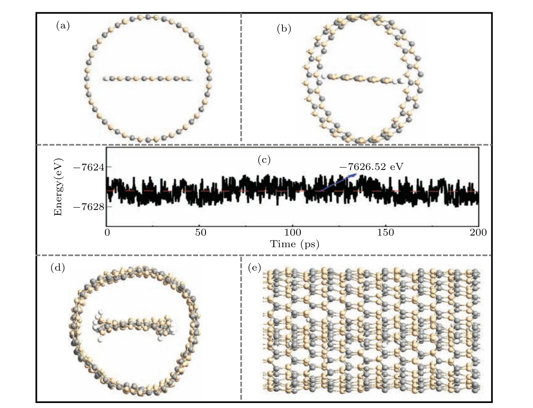
Fig.2. Schematic diagrams of(a)top view,(b)side view,(c)total energy evolution,[(d),(e)]snapshots of hybrid structure of SiCNTs/SiCNRs 1D vdWhs,obtained from molecular dynamics(MD)simulations in a time range of 200 ps.

Table 1. Bandgaps,VBMs,and CBMs of SiCNTs/SiCNRs 1D vdWhs.

Fig.3. Band structures of SiCNTs/SiCNRs 1D vdWhs: (a)(22,0)@A10,(b)(23,0)@A10,(c)(24,0)@A10,(d)(25,0)@A10,(e)(24,0)@A9,(f)(24,0)@A11,(g)(24,0)@A12,with green and brown lines indicating SiCNTs and SiCNRs,respectively.
As we already know, the applied electric field can effectively regulate the electronic structures of the vdW heterostructure. In this paper, two possible electric field directions are considered,i.e., perpendicular and parallel to the SiCNR.The electric field is applied in a range from 0 V/?A to 0.5 V/?A in steps of 0.1 V/?A.Figures 4 and 5 present the electronic structures of the SiCNTs/SiCNRs 1D vdWhsversusthe applied electric field. For perpendicular direction(see Fig.4),due to plane symmetrical structures of the SiCNTs/SiCNRs 1D vdWhs,the electric field’s positive and negative directions lead to the same results. Thus, only the positive direction of the electric field is given in the following. In a range of 0.1 V/?A to 0.3 V/?A,both the VBM and CBM are placed at theΓpoint,indicating that SiCNTs/SiCNRs 1D vdWhs are direct bandgap semiconductors. Furthermore, both the CBM and VBM mainly originate from the SiCNTs, demonstrating that SiCNTs/SiCNRs 1D vdWhs have unique type-I band alignment. When the electric field intensity is equal to 0.4 V/?A,the bandgaps are closed and change into metals. For parallel direction(see Fig.5),both the VBM and CBM are placed at theΓpoint in a range from?0.3 V/?A to 0.3 V/?A,indicating that SiCNTs/SiCNRs 1D vdWhs are direct bandgap semiconductors. Furthermore, both the CBM and VBM originate mainly from the SiCNTs,indicating the unique type-I band alignment of the SiCNTs/SiCNRs 1D vdWhs. When the electric field intensity is equal to or greater than 0.4 V/?A, the bandgaps are closed and change into metals. However, due to different edges of the SiCNRs,the bandgap and band-edge for negative electric field are not similar to those for positive electric field.According to the mentioned results, the SiCNTs/SiCNRs 1D vdWhs’electronic structures can be adjusted by applying electric fields.

Fig. 4. Band structures of SiCNTs/SiCNRs 1D vdWhs in the presence of electric fields under perpendicular direction in steps of 0.1 V/?A, with green and brown lines indicating SiCNTs and SiCNRs,respectively.
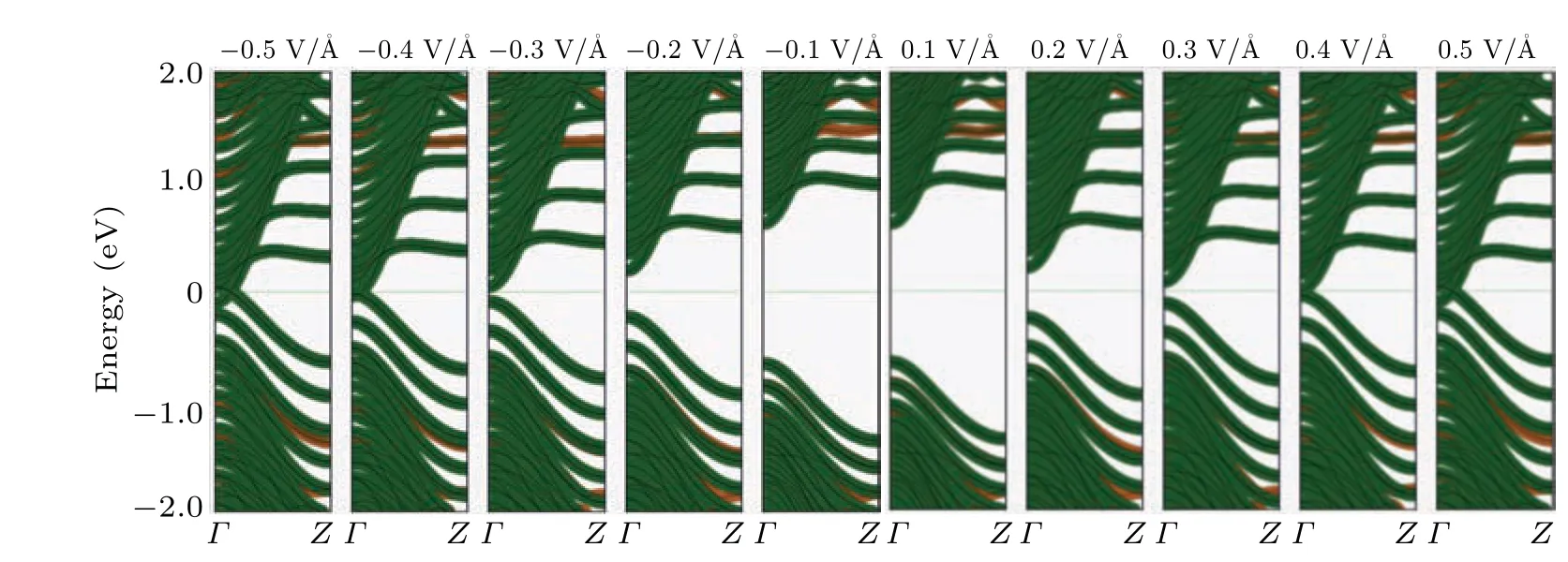
Fig.5. Band structures of SiCNTs/SiCNRs 1D vdWhs in the presence of electric fields under parallel direction in steps of 0.1 V/?A,with green and brown lines indicating SiCNTs and SiCNRs,respectively.
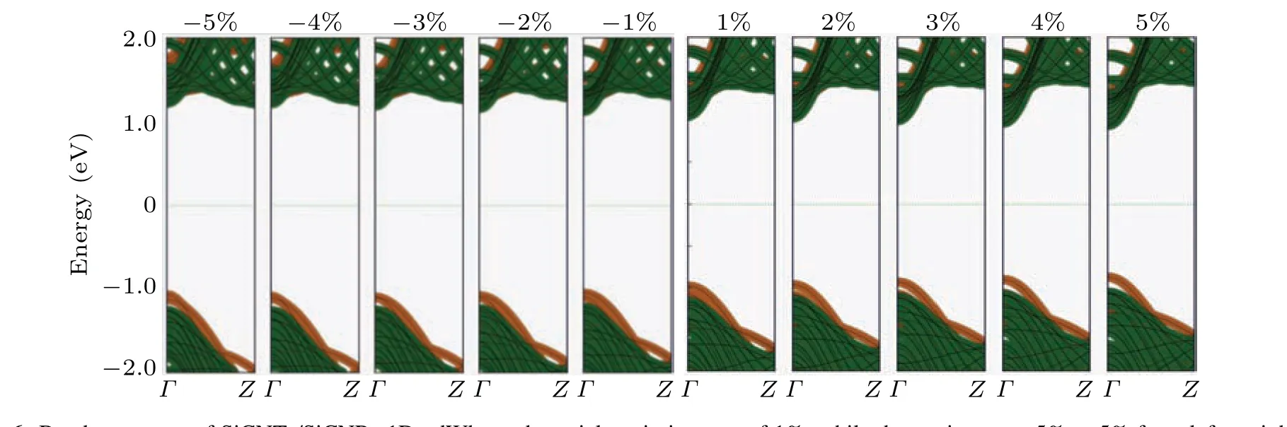
Fig.6. Band structures of SiCNTs/SiCNRs 1D vdWhs under axial strain in steps of 1%, while the strains are ?5%to 5%from left to right.The green and brown lines represent SiCNTs and SiCNRs,respectively.
According to previous theoretical and experimental results, the vdWhs’electronic structures can also be influenced by the strain. Thus, the influence of axial strain on the SiCNTs/SiCNRs 1D vdWhs’ electronic structures are verified.The crystal lattice parameters are changed to emulate the influence of axial strain on SiCNTs/SiCNRs 1D vdWhs, which can be obtained as follows:

wherea0andadenote the crystal lattice parameters under unstrained and strained situations, respectively. In this paper, (24, 0)@A10 is chosen as an example. The influences of strain on the band structures of the CNTs/GNRs 1D vdWhs are depicted in Fig.6. In the whole range of[?5%,5%],both the VBM and CBM are placed at theΓpoint within the twodimensional hexagonal Brillouin region, indicating a direct semiconductor. Besides, the VBM is extracted mainly from the SiCNRs,while the CBM is extracted from the SiCNTs,indicating that it is a typical type-II band alignment. According to the mentioned results, the (24, 0)@A10 is a direct semiconductor with a type-II band alignment under axial strain.Interestingly, it is found that both the bandgap and the bandedge have small changes,demonstrating the robust electronic structure of the SiCNTs/SiCNRs 1D vdWhs under axial strain.
4. Conclusions
In this work, MD simulation and first-principles computations are employed to verify the thermodynamic stability and electronic structures of SiCNTs/SiCNRs 1D vdWhs under electric fields and strain. The MD simulation founding demonstrates the stability structure of SiCNTs/SiCNRs 1D vdWhs under practical environmental conditions. According to the electronic structures calculated results,the type-II band alignment appears in SiCNTs/SiCNRs 1D vdWhs with different diameters. Furthermore,it is concluded that the bandgaps of SiCNTs/SiCNRs 1D vdWhs are closed at 0.4 V/?A.Besides,it is found that the SiCNTs/SiCNRs 1D vdWhs have a robust electronic structure under axial strain. The obtained results demonstrate that the SiCNTs/SiCNRs 1D vdWhs could provide a new way to the advanced electronics devices’growth.

- Chinese Physics B的其它文章
- Modeling the dynamics of firms’technological impact?
- Sensitivity to external optical feedback of circular-side hexagonal resonator microcavity laser?
- Controlling chaos and supressing chimeras in a fractional-order discrete phase-locked loop using impulse control?
- Proton loss of inner radiation belt during geomagnetic storm of 2018 based on CSES satellite observation?
- Embedding any desired number of coexisting attractors in memristive system?
- Thermal and mechanical properties and micro-mechanism of SiO2/epoxy nanodielectrics?