
Effect of nitrogen gas flow and growth temperature on extension of GaN layer on Si*
2021-11-23 07:31:56JianKaiXu徐健凱LiJuanJiang姜麗娟QianWang王茜QuanWang王權(quán)HongLingXiao肖紅領(lǐng)ChunFeng馮春WeiLi李巍andXiaoLiangWang王曉亮
Chinese Physics B 2021年11期
Jian-Kai Xu(徐健凱) Li-Juan Jiang(姜麗娟) Qian Wang(王茜) Quan Wang(王權(quán))Hong-Ling Xiao(肖紅領(lǐng)) Chun Feng(馮春) Wei Li(李巍) and Xiao-Liang Wang(王曉亮)
1Key Laboratory of Semiconductor Materials Science,Institute of Semiconductors,Chinese Academy of Sciences,Beijing 100083,China
2Center of Materials Science and Optoelectronics Engineering,University of Chinese Academy of Sciences,Beijing 100049,China
3School of Microelectronics,University of Chinese Academy of Sciences,Beijing 100049,China
4Beijing Key Laboratory of Low Dimensional Semiconductor Materials and Devices,Beijing 100083,China
5The State Key Laboratory of Crystal Materials,Shandong University,Jinan 250100,China
6Institute of Novel Semiconductors,Shandong University,Jinan 250100,China
Keywords: GaN extension,MOCVD,nitrogen flow,growth temperature
1. Introduction
GaN is an attractive material for application as highfrequency, high-power electronic devices, light-emitting diodes,and lasers,due to its wide band gap,high critical electric field strength, high electron saturation velocity, and high thermal stability.[1-6]Up to now,GaN compound semiconductor materials have received extensive attention.[7-14]Numerous studies have been conducted to determine the suitability of materials as substrates for GaN, such as GaN, SiC, sapphire,and Si.[15-21]Due to its cost-effectiveness,larger wafer diameter,higher thermal conductivity relative to sapphire,and the ability to integrate with mature Si-based processing technologies, Si is one of the best choices for substrates. However, the large lattice constant mismatch (?16.9%) and thermal expansion coefficient mismatch(56%)between GaN and Si substrate lead to high defect density and cracks.[22,23]Many groups have attempted to grow flat and crack-free GaN films in the past few decades with several methods, including the pre-deposition of Al on the Si surface, introduction of high temperature AlN(HT-AlN)buffer layers and adoption of stepgraded AlxGa1?xN interlayers. The pre-deposition of Al can effectively suppress the unnecessary formation of SiNx.[24]Introducing HT-AlN buffer layers compensates tensile stress in GaN and adopting step-graded AlxGa1?xN interlayers helps achieve a gradual change of lattice constants and thermal expansion coefficient from AlN to GaN.[17,25]
The quest for cost reduction promoted the continuous increase in the size of Si substrates for GaN epitaxial growth,while uniformity of the crystal quality of the large size Si wafer has also come out. There are few reports about the uniformity of the crystal quality of the GaN epitaxial layer on the Si substrate.In 2014,Pinoset al.[26]reported the coefficient of variation of the 9.1%GaN(0002)XRD rocking curve FWHM on a 6-inch Si substrate. In 2017,Jiet al.[27]reported a 2.4%coefficient of variation of epitaxial wafers of the same size. In this paper,we realize 6-inch Si substrate high quality flat and crack-free GaN epitaxial growth by MOCVD through increasing the nitrogen flow and increasing the growth temperature of HT-AlN and AlGaN buffer layers near the primary flat of the wafer. The GaN layer has extended more adequately on the Si substrate.
2. Experiments
In this study, the samples were grown on 6-in(1 in=2.54 cm) Si (111) substrates by our group’s selfmade metal-organic chemical vapor deposition (MOCVD).Trimethylgallium (TMGa), trimethylaluminum (TMAl), and ammonia were used as the precursors for Ga, Al, and N,respectively. The initial 1-mm-thick Si (111) substrate was heated to 1050°C in the hydrogen atmosphere and annealed for about 5 min. The Al predeposition was firstly carried out on the Si surface for 15 s to avoid the formation of amorphous SiNx. The buffer layers consisted of a 150-nm HT-AlN buffer layer and three step-graded AlxGa1?xN intermediate layers withx=0.75, 0.5, and 0.25. The growth conditions for AlN and AlGaN buffer layer are above 1000°C at a pressure of 75 Torr(1 Torr=1.33322×10²Pa). The outlet of the nitrogen flow gas is located in the center of the MOCVD gas/particle screening flange. The role of the nitrogen gas is to push various gases to the edge of the rotating wafer carrier. In the process of growing AlN and AlGaN layers,we adjusted different nitrogen flow rates for five samples named A-E(A:150 sccm,B: 200 sccm, C: 250 sccm, D: 350 sccm, E: 500 sccm). In samples F-I, in order to further relieve the tensile stress, an LT-AlN layer was grown between Al pre-deposition and HTAlN layer.[28-31]The growth temperature in HT-AlN and Al-GaN layers growing process near the primary flat of the wafers were changed from 1025°C to 1065°C for samples F-I.The detailed description of all the samples are listed in Table 1.The thicknesses of AlxGa1?xN layers were monitored byinsituinterferometer to be about 200 nm, 250 nm, and 300 nm for samples and then about 2-μm-thick GaN was overgrown on these buffers. The thickness of the layers was verified by Hitachi S-4800 scanning electron microscope(SEM).The crystalline quality of AlN and GaN layers were measured using PANalytical X’Pert PRO MRD(Malvern Panalytical,Almelo,The Netherlands). Olympus BX51M optical microscopy was used to characterize GaN surface morphologies.

Table 1. Detailed description of the nine samples.
3. Results and discussion
The deposition of all samples was monitored byin-situinterferometer,and the wavelength of the light source used for the reflectometry was 900 nm. Figure 2(a) shows the typical trace of thein-situoptical reflectivity during MOCVD growth.The growth stages corresponding to Fig.2(a)are(i)HT-AlN,(ii)AlGaN-1 layer,(iii)AlGaN-2,(iv)AlGaN-3,and(v)GaN layers. The stage between(iv)and(v)is a conversion process from AlGaN growth to GaN growth. Figure 2(b) is a crosssectional view of the epitaxial structure measured by SEM,and it is clear that the thickness of each layer is quite close to the designed epitaxial structure of Fig.1. Additionally,during the epitaxial process,the substrate revolves around the center of the rotating wafer carrier at high speed with the primary flat of the substrate perpendicular to the radial direction of the rotating wafer carrier. Therefore, we selected 5 locations including the center point in the direction perpendicular to the primary flat on the wafer which is shown in Fig.3.

Fig.1. Schematic structure of the samples grown.
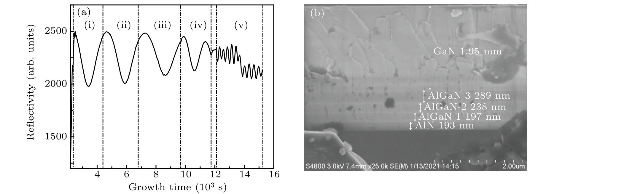
Fig. 2. (a) Typical traces of in-situ optical reflectivity at different growth stages, which are separated by dot lines: (i) AlN buffer, (ii)-(iv)AlGaN buffer,and(v)GaN epilayer. (b)Cross-sectional SEM images of the epilayers.

Fig.3. Locations on top of the samples.
Firstly,we studied the influence of different nitrogen gas flow rates on the extension of GaN on Si substrate. Figure 4 displays images of sample A to sample E after growth. It can be seen that each sample has two distinct areas, a bright area and a dark area. At the same time,with the increase of nitrogen flow rate,the bright areas increased significantly,while the dark area decreased.Further,figure 5 shows that the surface of the epitaxial wafer is observed through an optical microscope,and it is found that the surface of the bright area has no cracks,but the surface of the dark area is very rough. By increasing the nitrogen flow rate,the crack-free area on the surface of the epitaxial wafer gradually enlarged,and the rough area reduced to close to the primary flat. This indicates that increasing the nitrogen flow rate can effectively improve the extension of the epitaxial layers.

Fig.4. The images of sample A(a),sample B(b),sample C(c),sample D(d),and sample E(e).

Fig.5. Optical microscopy views of(a)surface without cracks(bright area of the wafer in Fig.4)and(b)rough surface(dark area of the wafer in Fig.4).
It was proposed that adatom diffusion was considered to be responsible for the material quality and surface morphology.[32]During the growth of the epitaxial layers,nitrogen gas accelerates the precursor along the surface of the wafers and its pump out from the gas outlet near the edge of the rotating wafer carrier. As N2participates in the mixing of the reaction gases,the concentration of the reactants decreases,which reduces the speed of epitaxial growth. Increasing nitrogen gas flow may leads to the lower growth rate. Throughin-situinterferometer,we can get the total growth time of the AlN layer and three AlGaN layers on Si substrate under different nitrogen flow rate conditions,which is shown in Fig.6.Consistent with the above discussion,under the same epitaxial thickness,as the nitrogen flow rate increases,the total growth time of the AlN layer and the three AlGaN layers gradually increases. The lower growth rate allows more time to diffuse on the surface of the epitaxial layers, which was considered to be responsible for the material quality and surface morphology.[30]Flat and high quality AlN and AlGaN buffer layers can be the precondition of GaN growth.

Fig. 6. Total growth time of AlN and three AlGaN layers on location(0,?40)of all samples with different nitrogen flow rates.
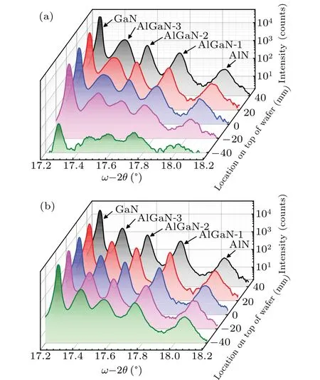
Fig.7. XRD ω-2θ scan plots of GaN(0002)to AlN(0002)reflection of sample A(a)and sample E(b).
Figures 7(a) and 7(b) show the XRDω-2θscan results of the epitaxial layer at different positions on sample A (nitrogen flow rate of 150 sccm) and sample E (nitrogen flow rate of 500 sccm), respectively. The diffraction peaks correspond to GaN,AlGaN-3,AlGaN-2,AlGaN-1,and AlN in the order from left to right. And the black, red, blue, pink, and green curves correspond to the x-rays diffraction results at the positions (0, 40), (0, 20), (0, 0), (0,?20), (0,?40) on the epitaxial wafer, respectively. When the nitrogen flow rate is 150 sccm, as shown in Fig. 7(a), the closer the test point to the primary flat, the weaker the diffraction peak intensity of the HT-AlN layer and the three AlGaN layers, especially the position (0,?40). At the same time, the diffraction peaks of each layer at the test point near the primary flat are not as sharp as the location far from the primary flat. It indicates that, in the wafer, the crystal quality distribution of the epitaxial layer is uneven along the direction perpendicular to the primary flat. When the flow rate increased to 500 sccm, the crystal quality distribution of the epitaxial layer is more uniform along the direction perpendicular to the primary flat,and the diffraction peaks are sharper for the HT-AlN and three Al-GaN layers at each position of the wafer, as can be seen in Fig. 7(b). Therefore, a higher nitrogen flow rate is beneficial to improve the uniformity of the epitaxial layer crystal quality on the Si substrate, which is consistent with the results of optical microscopy.
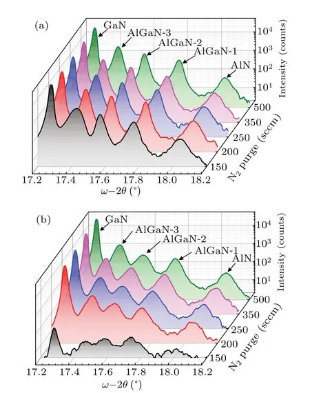
Fig.8. XRD ω-2θ scan plots of GaN(0002)to AlN(0002)reflection of all samples on location(0,40)(a)and location(0,?40)(b).
Further, the effect of nitrogen flow rate on the material quality at different positions on the epitaxial wafer is also studied. Figures 8(a) and 8(b) displays the XRDω-2θscan results on the wafer at locations far away from the primary flat (0, 40) with that near the primary flat (0,?40), respectively. The diffraction peaks correspond to GaN, AlGaN-3,AlGaN-2,AlGaN-1,and AlN in order from left to right. The black, red, blue, pink, and green curve correspond to the xray diffraction results under the nitrogen flow conditions of 150 sccm, 200 sccm, 250 sccm, 350 sccm, and 500 sccm,respectively. With the increase of nitrogen purge flow rate(150 sccm→500 sccm),the diffraction peak intensities of each epitaxial layer does not change significantly at the position(0,40) which is far away from the primary flat. However, at the position(0,?40)near the primary flat,the diffraction peak intensities of the HT-AlN layer and the three AlGaN layers are increased with the increase of the nitrogen flow.This indicates that increasing the nitrogen flow rate can significantly improve the material quality near the primary flat on the epitaxial wafer,and thus a more uniform material.
In order to more intuitively characterize the effect of different nitrogen flow rate on the crystal quality of the epitaxial layers on the Si substrate, we performed an XRDωrocking scan at different positions on the samples A-E. As shown in Fig. 9(a), as the nitrogen purge flow rate increases, for samples A-E,the(0002)FWHM value of the AlN epitaxial layer is more consistent in the direction perpendicular to the primary flat,indicating a more uniform AlN crystal quality. And the significant improvement of the AlN crystal quality located close to the primary flat may account for it. The high crystal quality uniformity of AlN epitaxial layer is an important foundation for GaN epitaxial growth. From Fig.9(b),with the increase of nitrogen purge flow rate,for samples A-E,the(0002)FWHM value of the GaN epitaxial layer near the primary flat exhibits a considerable decrease. The crystal quality uniformity of the GaN epitaxial layer in the direction perpendicular to the primary flat has been improved,which is consistent with AlN epitaxial layer.

Fig.9. (a)AlN(0002)and(b) GaN(0002)XRD FWHMs of samples A-E of different locations on the surface.
In order to further improve the extension of the GaN layer,growth temperature of HT-AlN and AlGaN layers near the primary flat of the wafers were changed from 1025°C to 1065°C for samples F-I.Figure 10 shows the images of samples F-I.By increasing the local growth temperature of AlN and Al-GaN buffer layers near the primary flat,the crack-free area on the surface of the epitaxial wafer gradually enlarged, and the rough area reduced significantly,which is shown in Fig.10(i).For samples F-I,the sizes of the crack-free area are 129.1 cm2,146.3 cm2,159.1 cm2,and 168.6 cm2,respectively.Therefore,increasing the growth temperature can effectively improve the extension of the epitaxial layers.

Fig.10. The images of sample F(f),sample G(g),sample H(h),sample I(i).
It was proposed that with the increase of the temperature,the AlN nucleation probability increases,and the grain size decrease rapidly,so there is a more uniform and flat AlN buffer layer surface,as well as improved quality of AlN crystals.[33]XRDωrocking scan at different positions on the samples F-I has been measured and the result was shown in Fig. 11.With the increasing of the growth temperature near the primary flat of the wafers, as shown in Fig. 11(a), the (0002)FWHM value of the AlN epitaxial layer has been decreased.The (0002) FWHM value of the GaN has further decreased which is shown in Fig. 11(b). The variation of the (0002)FWHM value of the GaN has dropped to 2.3%. We can conclude that the crystal quality near the primary flat has been notably improved. Therefore,the crystal quality uniformity of the epitaxial layer in the direction perpendicular to the primary flat has been improved by indeed increasing the local growth temperature.
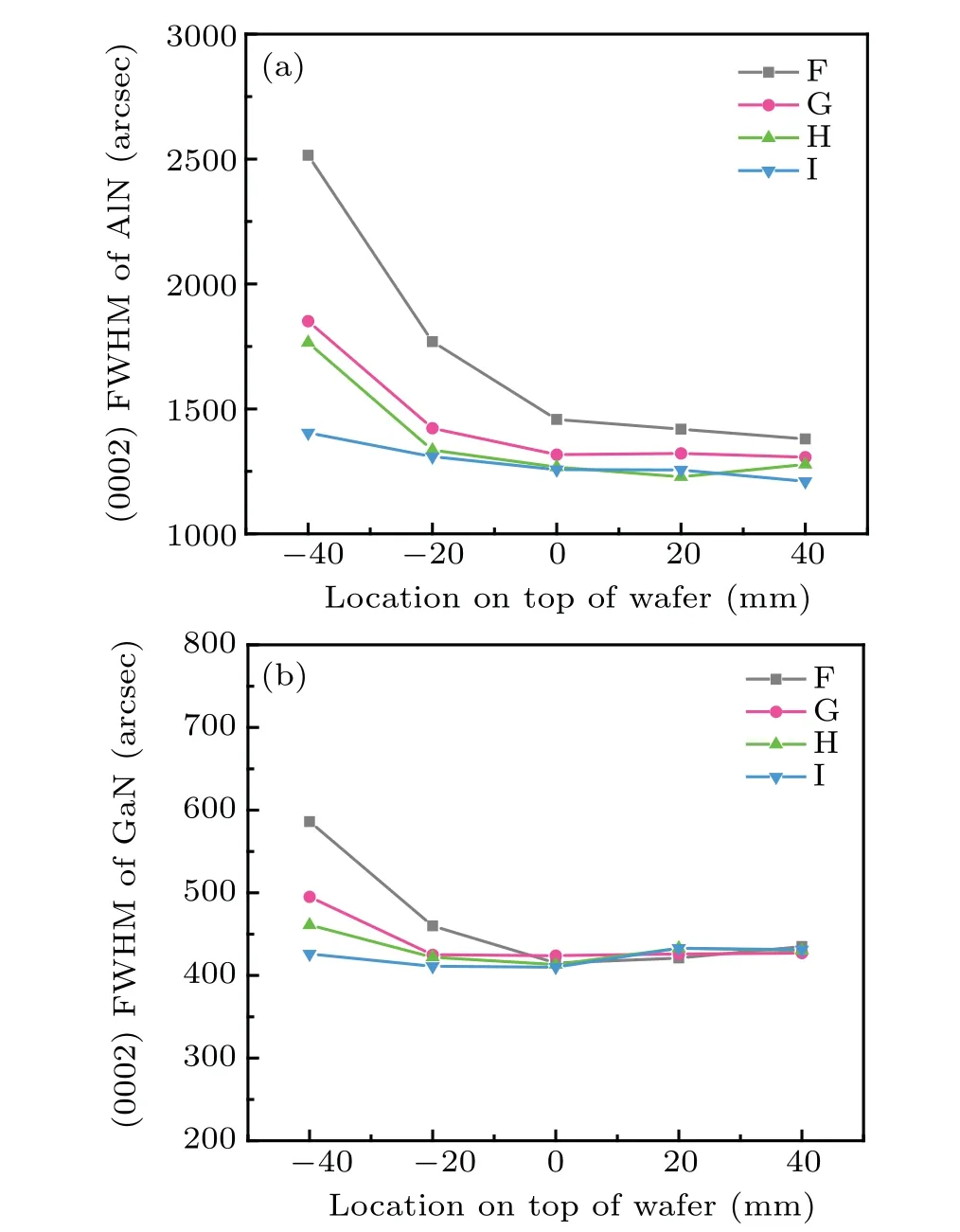
Fig.11. (a)AlN(0002)and(b)GaN(0002)XRD FWHMs of samples A-E of different locations on the surface.
4. Conclusion
In this research,we adjusted the nitrogen flow rate and the local growth temperature near the primary flat of the wafers to study the influence on extension of GaN epitaxial layers on Si substrates. By increasing the nitrogen flow rate and the local growth temperature near the primary flat of the wafers,we have found that the crack-free area on the surface of the epitaxial wafer gradually enlarged,and the rough area reduced to close to the primary flat and at the same time,the crystal quality uniformity has been improved. This research provides an effective method for extension of GaN epitaxial layer growth on Si substrates.
猜你喜歡
美與時(shí)代·城市版(2024年10期)2024-12-31 00:00:00
Plasma Science and Technology(2022年9期)2022-08-29 00:42:50
中國藏學(xué)(2022年1期)2022-06-10 05:55:08
歷史教學(xué)問題(2021年4期)2021-11-05 07:02:08
藝術(shù)品鑒(2021年3期)2021-04-24 07:53:52
美與時(shí)代·美術(shù)學(xué)刊(2020年3期)2020-06-29 07:24:35
作文大王·笑話大王(2019年5期)2019-06-09 20:13:56
愛你·心靈讀本(2018年8期)2018-09-10 04:10:32
愛你(2018年22期)2018-08-17 03:06:00
新高考·高一物理(2016年3期)2016-05-18 17:11:22
- Chinese Physics B的其它文章
- Erratum to“Floquet bands and photon-induced topological edge states of graphene nanoribbons”
- Viewing the noise propagation mechanism in a unidirectional transition cascade from the perspective of stability*
- Nonlinear signal transduction network with multistate*
- Optical strong coupling in hybrid metal-graphene metamaterial for terahertz sensing*
- Any-polar resistive switching behavior in Ti-intercalated Pt/Ti/HfO2/Ti/Pt device*
- Magnetic two-dimensional van der Waals materials for spintronic devices*