
Band offsets and electronic properties of the Ga2O3/FTO heterojunction via transfer of free-standing Ga2O3 onto FTO/glass*
2021-11-23 07:28:10XiaWang王霞WeiFangGu古衛(wèi)芳YongFengQiao喬永鳳ZhiYongFeng馮志永YueHuaAn安躍華ShaoHuiZhang張少輝andZengLiu劉增
Chinese Physics B 2021年11期
Xia Wang(王霞) Wei-Fang Gu(古衛(wèi)芳) Yong-Feng Qiao(喬永鳳) Zhi-Yong Feng(馮志永)Yue-Hua An(安躍華) Shao-Hui Zhang(張少輝) and Zeng Liu(劉增)
1Department of Electrical Engineering and Automation,Shanxi Institute of Technology,Yangquan 045000,China
2School of Optoelectronic Engineering,Guangdong Polytechnic Normal University,Guangzhou 510665,China
3Shenzhen Engineering Laboratory of Phosphorene and Optoelectronics,International Collaborative Laboratory of 2D Materials for Optoelectronics Science and Technology of Ministry of Education,College of Optoelectronic Engineering,Shenzhen University,Shenzhen 518060,China
4College of Electronic and Optical Engineering&College of Microelectronics,Nanjing University of Posts and Telecommunications,Nanjing 210023,China
5National and Local Joint Engineering Laboratory for RF Integration and Micro-Packing Technologies,Nanjing University of Posts and Telecommunications,Nanjing 210023,China
Keywords: Ga2O3/FTO heterojunction,band alignment,magnetron sputtering,free-standing
1. Introduction
Oxide semiconductors are always regarded as important materials due to their optical transparency, high mobility and mature preparation technologies, catering for many applications,and have been developed in scientific and technological fields of photonic and optoelectronic devices.[1]In an oxide system, the band alignment of the oxide heterojunction plays a very important role in governing the functional electronic devices,since the device performances are seriously affected by the carrier transport at the heterogeneous interfaces.[2,3]
Over the last two decades, Ga2O3, a very important and promising oxide semiconductor material, has become a candidate in the fabrication of solar-blind UV photodetectors,high-power electronics, and radiation-resistant optoelectronics, which are benefited by its ultra-wide bandgap (Eg~5 eV) and high breakdown critical electrical field (Ebr~8 MV/cm).[4-6]The band offsets at conduction and valence band edges are very important to guide the design of heterogeneous devices. To date, there are a few studies on the band alignments of Ga2O3-based heterojunctions,[7]and they have increased significantly in the last 2-3 years.For instance,Raoet al.researched the band offsets of p-type oxide (SnO or NiO)/Ga2O3heterojunctions.[8]Zhiet al.studied the band offsets of the In2O3/Ga2O3heterointerface.[9]The band alignments of the ZnO/Ga2O3and Ta2O5/Ga2O3heterointerface were studied by Liuet al.[10]The various alignments lead to different functional operations on the basis of the alignment results. In brief,the fabrication of oxide heterojunctions based on Ga2O3at the interface can provide new possibilities to develop oxide heterostructured(opto)electronics.[3,7,11,12]
F-doped SnO2(FTO)has inspired interest for use in transparent conductive electrodes (TCEs), transparent optoelectronic devices and flexible display technologies,due to its low cost and strong stability.[13]In comparison, Sn-doped In2O3(ITO)conducts electricity well;[14]however,the ITO films exhibit brittleness, poor stability at high temperature and high costs due to the presence of indium.[15]Therefore, as a replacement for ITO, FTO has a wide range of applications in constructing electrodes,and sensing and switching devices.[16]
Considering the applications of Ga2O3in flexible and transparent optoelectronic devices[17]and the meanings of band alignment for the development of Ga2O3based heterogeneous electronic and optoelectronic devices,[11,18,19]it is necessary to study the band calibration of the Ga2O3/FTO heterojunction. The band alignment of the Ga2O3/FTO heterojunction can provide a reference for the application of Ga2O3/FTO heterojunctions in transparent optoelectronic devices and flexible devices.
In this paper,we construct the Ga2O3/FTO heterojunction using radio-frequency (r.f.) magnetron sputtering and freestanding film transfer techniques. Then,the band alignment of the Ga2O3/FTO heterojunction is determined using x-ray photoelectron spectroscopy(XPS)and an ultraviolet-visible(UVVis)absorbance spectrum. Finally,the electronic properties of the Ga2O3/FTO heterojunction are shown and discussed.
2. Experimental details
To obtain the band alignment of the Ga2O3/FTO heterojunction, three samples were prepared. The detailed experimental processes are given as follows.
Firstly,three commercially available FTO substrates were cleaned with acetone,ethyl alcohol and deionized water in the appropriate order using an ultrasonic cleaning machine, then dried with a N2flow gun.
Secondly,two FTO substrates were used as substrates to deposit Ga2O3by r.f.magnetron sputtering for about 100 min and 1 min,respectively.Thus,three samples,i.e.,(i)FTO substrate,(ii)~300 nm Ga2O3on FTO substrate and(iii)<5 nm Ga2O3on FTO substrate,were finished by fabrication. During deposition,the basic pressure is~2×10?4Pa,and the Ga2O3thin film is deposited at argon pressure of 0.8 Pa and r.f.power of 70 W.
Thirdly, according to Kraut’s method,[20,21]the bonding states of Ga2O3and FTO can be determined by XPS scanning data. The charge-shift spectra were calibrated with the adventitious C 1s peak at 284.9 eV.The optical bandgap of FTO was determined by the UV-Vis absorption spectrum and the optical bandgap values of Ga2O3have been reported in our previous works.[22,23]
Finally,the Ga2O3/FTO heterojunction on the FTO/glass substrate was fabricated by transferring free-standing Ga2O3film (the detailed experimental descriptions can be seen in Ref.[22]),since high-quality Ga2O3films need to be prepared at 750°C, which will change the existence of the FTO film(destroy over 550°C).[23]The current-voltage (I-V) characteristic curves were tested by a Keithley 2450 semiconductor analysis meter. The photocurrent measurement was performed under 254 nm UV light illumination with intensity of 300μW/cm2.
3. Results and discussion
Figure 1(a) shows the UV-Vis absorbance spectrum of the FTO thin film and the plot of [(αhv)2versushv] is displayed in Fig. 1(a) inset. The bandgap (Eg) of FTO is estimated to be 4.0 eV according to the results in Fig.1(a)inset,which is comparable to the reported values. TheEgof Ga2O3is about 4.75 eV, which has been described in our previous reports.[22]As the FTO substrate is commercially available,it is necessary to verify the quality of the transferred Ga2O3. As shown in Fig. 1(b), the high-resolution transmission electron microscopy(HR-TEM)image suggests that the free-standing Ga2O3film is polycrystalline.[22]
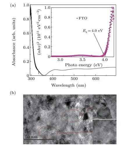
Fig.1. (a)The UV-Vis absorbance spectrum of FTO;the inset is the plots of[(αhv)2 versus hv],hv is the incident photon energy and α is the absorbance coefficient. (b)The HR-TEM image of the free-standing Ga2O3 film.
Figures 2(a) and 2(c) show the valence band minimums(VBMs)for the FTO and Ga2O3,respectively. And the highresolution XPS spectra of the core energy levels for the FTO and Ga2O3are shown in Figs. 2(b) and 2(d), from which we can see that the VBMs of the FTO and Ga2O3are 2.3 eV and 1.9 eV, respectively; the core energy levels of the FTO and Ga2O3are provided with the values of 494.95 eV and 1118.63 eV. Figures 2(e) and 2(f) show the core energy levels of the Ga2O3/FTO heterojunction in the XPS spectra. The values of the core energy levels of the Ga2O3and the FTO are 1118.34 eV and 491.85 eV at the Ga2O3/FTO heterointerface,respectively. Based on these binding energy values, the ?ECand ?EVof the Ga2O3/FTO (GAO/FTO) heterojunction can be calculated using the following equations.[10,20,21]

Table 1. Values of core energy levels,VBMs and band offsets in this experiment(eV).
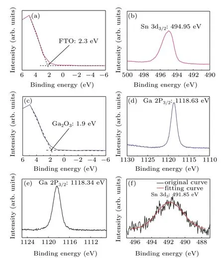
Fig. 2. XPS spectra of (a) VBM of FTO, and (b) the Sn 3d3/2 core energy level. XPS spectra of(c)VBM of Ga2O3,and(d)the Ga 2p3/2 core energy level. (e)Ga 2p3/2 core energy levels,and(f)XPS spectra of Sr 3d3/2 at the Sr3Al2O6/Ga2O3 interface.
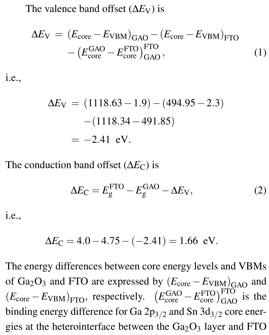
Figure 3(a)shows the diagram of the energy band alignment of the Ga2O3/FTO heterojunction. The ?EVof the heterojunction is?2.41±0.02 eV and ?ECis 1.66±0.02 eV in the operating hetero-structured devices,[25-27]allowed with deviations from measurement and calculation. Figure 3(a) suggests a staggered type-II energy band alignment of the Ga2O3/FTO heterojunction. The staggered type-II Ga2O3/FTO heterojunction misses the hole confinement.[10]The valence band offset and the conduction band offset are both greater than 1 eV, suggesting a large enough band offset for the successful fabrication of the heterojunction with rectification properties.[28]The obtained band offsets of the Ga2O3/FTO heterojunction are helpful for theoretical correction. Furthermore, it is worth noting that the heterojunction prepared here, unlike the high-temperature deposited heterojunction, does not have dense bonding, and may have space charge and/or an air insulating layer across the heterogeneous interface.
To explore the volt-ampere characteristics of the Ga2O3/FTO heterojunction, indium (In) electrodes are mechanically transferred onto the surfaces of FTO and Ga2O3,respectively. Figures 4(a) and 4(b) show a schematic diagram and a photograph of the Ga2O3/FTO heterojunction. In Fig. 4(c), the linear scaleI-Vcurves of the Ga2O3/FTO heterojunction in the dark and under 254 nm UV light illumination are shown. It can be seen that the Ga2O3/FTO heterojunction presents rectified behavior, due to the discrete conduction band edges along with the large ?ECof 1.66 eV, as displayed in Fig.3(b).Moreover,compared with the dark conditions,the rectification characteristics are increased under the ultraviolet light illumination of 254 nm; during this step the photo-generated electron-hole pairs are excited,the electrons move to the conduction band,while the holes correspondingly appear at the valence band, leading to an enhancedI-Vperformance under illumination. The log-scaleI-Vcurves are presented in Fig. 4(d). The performance of the heterojunction is improved under 254 nm UV irradiation compared with that under dark conditions under conditions where the heterojunction interface is not treated by any physical or chemical techniques.
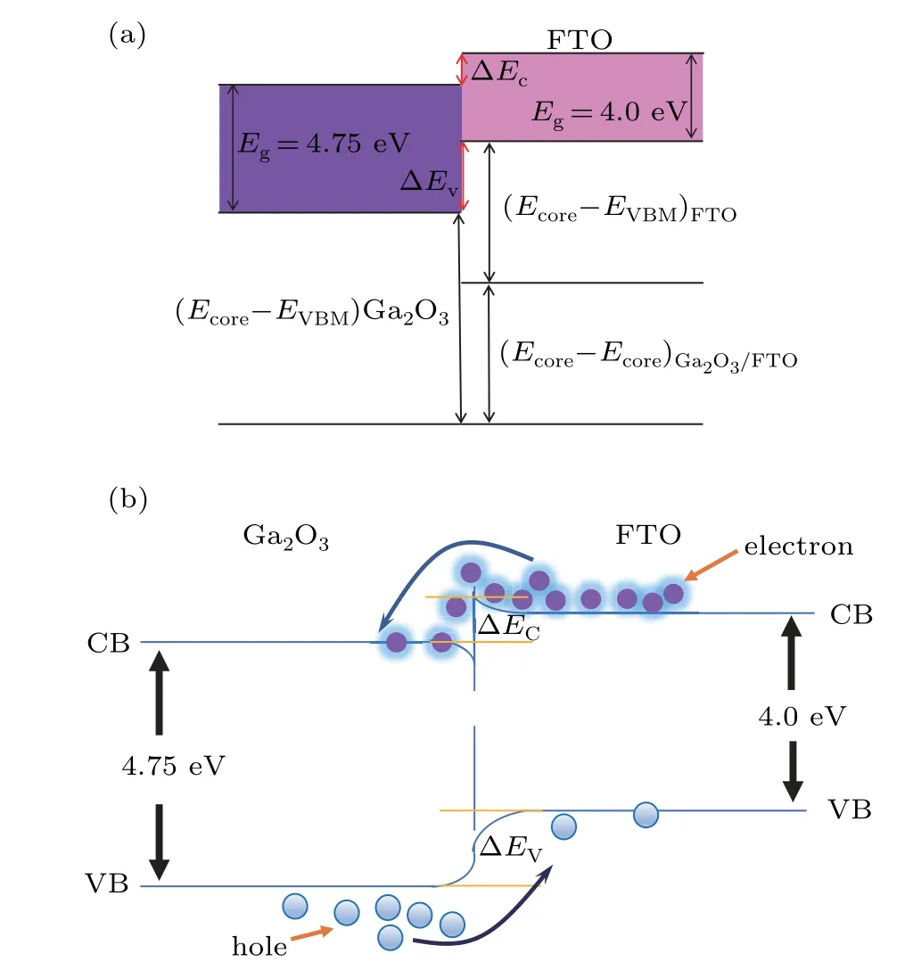
Fig. 3. The energy-band alignment diagram of the Ga2O3/FTO heterojunction.

Fig. 4. The Ga2O3/FTO heterojunction on glass substrate: (a) a schematic diagram; (b) a photograph; (c) the linear scale I-V characteristics; and (d)the log-scale I-V characteristics.
In short, the work reported in this paper shows the feasibility of preparing a Ga2O3/FTO heterojunction. In addition, higher rectification performance of the Ga2O3/FTO heterojunction can be obtained using effective interior interface treatments and improved growth techniques. This is because the magnetron sputtering method always causes damage to the films, which may lead to metal contaminants and interfacial disorder.[29,30]Finally,in this work,the rectifying characteristics of the Ga2O3/FTO heterojunction were verified.
4. Conclusion
Based on Kraut’s method, the band alignment of the Ga2O3/FTO heterojunction is studied using XPS in this paper. In particular, the Ga2O3/FTO heterojunction exhibits a staggered type-II band alignment accompanied with ?ECof 1.66±0.02 eV and ?EVof?2.41±0.02 eV.At the same time,the rectification ratio of the heterojunction was measured under the conditions of 254 nm light illumination and darkness.Based on the above results, some conclusions can be drawn from the Ga2O3/FTO heterojunction studied here with good rectifying behavior,and it is expected to be further applied to hetero-structured optoelectronic and electronic devices.
- Chinese Physics B的其它文章
- Erratum to“Floquet bands and photon-induced topological edge states of graphene nanoribbons”
- Viewing the noise propagation mechanism in a unidirectional transition cascade from the perspective of stability*
- Nonlinear signal transduction network with multistate*
- Optical strong coupling in hybrid metal-graphene metamaterial for terahertz sensing*
- Any-polar resistive switching behavior in Ti-intercalated Pt/Ti/HfO2/Ti/Pt device*
- Magnetic two-dimensional van der Waals materials for spintronic devices*