
Synthesis of SiC/graphene nanosheet composites by helicon wave plasma*
2021-07-30 07:39:34JiaLiChen陳佳麗PeiYuJi季佩宇ChengGangJin金成剛LanJianZhuge諸葛蘭劍andXueMeiWu吳雪梅
Chinese Physics B 2021年7期
Jia-Li Chen(陳佳麗) Pei-Yu Ji(季佩宇) Cheng-Gang Jin(金成剛)Lan-Jian Zhuge(諸葛蘭劍) and Xue-Mei Wu(吳雪梅)
1School of Physical Science and Technology and Collaborative Innovation Center of Suzhou Nano Science and Technology,Soochow University,Suzhou 215006,China
2The Key Laboratory of Thin Films of Jiangsu Province,Soochow University,Suzhou 215006,China
3Laboratory for Space Environment and Physical Sciences,Harbin Institute of Technology,Harbin 150001,China
4Analysis and Testing Center,Soochow University,Suzhou 215123,China
Keywords: helicon wave plasma,SiC/graphene nanosheet,x-ray photoelectron spectroscopy(XPS),fluorescence
1. Introduction
Silicon carbide (SiC) is a novel composite material with superior properties such as low density, high hardness,high strength, chemical inertness, high thermal conductivity(3 W/cm·K-5 W/cm·K) and a high breakdown field strength(2.0 MV/cm).[1,2]Many published reports covered the synthesis of nanocrystalline SiC and studying its photoluminescence (PL) properties.[3-5]SiC offers a unique combination of structural and electrical characteristics for applications in harsh environments such as high temperature and complex electromagnetic fields. Silicon carbide nanocrystals(SiC NCs) also show some properties beneficial to biological/photoelectric applications[5,6]and catalytic applications(including water decomposition and water purification).[7]Recently, many techniques such as sputtering, chemical vapor deposition (CVD),[8]plasma-enhanced chemical vapor deposition (PECVD), and ion implantation have been used for preparing SiC films.
Graphene is considered an incredibly strong material with large surface areas as well as excellent mechanical, optical,thermal, and electrical properties.[9]Many graphene-based materials have has shown to possess excellent performance in sensors,transistors,actuators,and storage devices.[10-13]
To our knowledge, few researches reported that tetramethylsilane (TMS) had been used as a source to synthesize SiC/GNSs in one step. The TMS is a simple organosilane and is widely used as a precursor for the synthesis of many important materials,[14-16]such as SiC nanoparticles,[17]and nanocrystals(NCs).[18]Welzelet al.[19]studied TMS as a precursor for the preparation of Si-C-N:H films by using an electron cyclotron resonance(ECR)plasma. Haqet al.[20]studied the growth of SiC nanocrystals by dissociation of TMS under atmospheric pressure microplasma. In particular,PECVD has been widely used to prepare various nanomaterials.It is worthwhile to note that the properties of the films are dependent on the preparation process. The helicon wave plasma(HWP)source can be widely used for preparing the nanomaterials,because of its high ionization rate,low deposition pressure,and high plasma density(≥1019m-3).[21]
In this work,we report a method of rapidly synthesize the SiC/GNS composites in one step by using high-density helicon wave plasma(HWP)technology and TMS as a precursor for the first time. We studied the microstructure as well as the growth model of the SiC/GNS structure.
2. Experiment
The SiC/GNSs were deposited on silicon (Si) substrates in an argon helicon wave plasma chemical vapor deposition(HWP-CVD)system using tetramethylsilane(TMS).Figure 1 shows a schematic diagram of the deposition system. The detailed equipment of the system has been reported elsewhere.[22,23]In this experiment, a p-Si (100) signal crystal was chosen as the substrate material. The substrates were cut into 1 cm×1 cm pieces and sequentially cleaned ultrasonically with acetone,alcohol and deionized water to remove impurities from the Si surface. The Si substrates were placed in the deposition chamber and secured, then the vacuum chamber was pumped to the background vacuum. After evacuation,Ar (99.99%) gas was introduced into the discharge chamber.In the axial magnetic field environment, the radio frequency modulation was used for Ar HWP discharge to clean the vacuum chamber,substrate and Si substrate. The HWP was generated by 1500 W, 13.56 MHz, RF power supply through an antenna at a pressure of 0.06 Pa and a static axial magnetic field of 1480 Gs (1 Gs=10-4T) in Ar as the working gas.The injected TMS was decomposed by Ar (40 sccm) HWP.The HWP discharge and the TMS input were turned off after ten min.

Fig.1. Schematic diagram of HWP-CVD experimental setup.
The morphologies of the SiC/GNSs were studied by scanning electron microscopy (SEM, Model Hitachi SU8100).X-ray photoelectron spectroscopy (XPS, Thermo ESCALAB 250 XI) analyzed the composition of the SiC/graphene composite nanosheets. The x-ray diffraction(XRD)patterns were obtained by using an x-ray diffractometer (Rigaku D/MAX-2000 PC). Raman spectra were measured with a Horiba Raman system and a 514-nm excitation semiconductor laser.Steady-state fluorescence(PL,FLS 920)was measured by using an OSRAM XBO 450-W high-pressure xenon arc lamp as a light source and showed a strong continuous spectrum in a range of 200 nm-900 nm. In the measurement, the working current and voltage were 25 A and 20 V, respectively the starting voltage was 25 kV, and the pressure was 5 atm(1 atm=1.01325×10⁵Pa).The optical emission spectra(OES)were collected with a grating spectrometer(MS 5204i)in combination with a 74-UV silica collimating lens.
3. Results and discussion
3.1. Structure and phase composition
Figure 2(a) shows a low magnification SEM image of SiC/GNS composites deposited for 10 min. It shows the nanosheets uniformly aggregated in a small island, like hairballs, with an average size of approximately 230 nm.Compared with a typical carbon nanosheet (vertically standing nanowalls with a maze-like, highly branched and porousstructure),[24]the SiC/GNS composites display some of those typical characteristics, such as vertically standing nanowalls with a maze-like structure. However, they aggregated into uniform spherical objects.

Fig. 2. (a) SEM of SiC/GNS composites and local enlargements; (b) XRD pattern of SiC/GNS composites.
Figure 2(b)shows the XRD[25]pattern of SiC/GNS composites.The major crystalline phases in the samples areα-SiC andβ-SiC.[26]The XRD pattern of the sample shows mainly cubic 3C-SiC (namely,β-SiC), crystalline phase of strong peaks corresponding to the (111), (220), and (311) planes.These values are consistent with those in the literature.[27]There also exist 2H-SiC (namely,α-SiC) peaks at 2θ=39.73°, 45.68°, and 66.54°. Theα-SiC peaks are weaker than theβ-SiC peaks. In this paper,[28]it is pointed out that the structure changes fromβ-SiC (cubic structure) toα-SiC(hexagonal structure) after cooling from high temperature of over 1500°C in Ar atmosphere. Theβ-SiC structure has been considered to be the low-temperature polymorph of SiC. In addition, weak hexagonal SiC peaks of (101) were observed,which are due to the polymorphic phase transition of cubic SiC formed by the reaction in HWP. In addition toα-SiC andβ-SiC, the phases such as graphite and silicon oxynitride were also identified. A carbon peak at 2θ=78.54°was observed.[29]The presence of silicon oxynitride was attributed to the contamination of oxygen during film preparation.

Fig.3. Raman spectra of SiC/GNS composites.
Raman spectra in Fig. 3 further confirm the structural characteristics of these materials. Each Raman band is analyzed by being fit with a Lorentzian line. The D-band seen in Fig. 3 is attributed to the strong peak carbon structure at 1355 cm-1.The mixed peak deconvolution is divided into two small peaks at 1592 cm-1and 1621 cm-1,which correspond to the G-band and D′-band, respectively. The D′was associated with six-membered ring structures and graphene edges,and D originates from disordered carbon, the G peak comes from the graphitized carbon.[29]The most prominent feature of graphene in Raman spectrum is the 2D peak; its position and shape are clearly distinguished among single-layer, doublelayer, and multi-layer graphene.[31,32]Single-layer graphene sheet has a single, clear 2D peak below 2700 cm-1.[33,34]The double-layer graphene sheet has a wider, upshifted 2D peak below 2700 cm-1.[31,32]Sheets with more than five layers and larger pieces of graphite exhibit similar spectra[31,32]with broad 2D peaks shifting up field above 2700 cm-1. The position and shape of the G peak further prove the graphene structure of the SiC/GNS composites. Listed in Table 1 are the full widths at half maximum(FWHM)and relative intensity ratios of band-peaks of D, G, D′, and 2D (ID/IG,ID′/IG,andI2D/IG) for the Raman spectra in Fig. 3. The large value ofID/IGindicates that the as-grown carbon material possesses a large number of defects,which are caused by vacancies,deformations, ripples and edges. The most important feature in Raman spectrum of graphene is 2D peak,and its intensity and position are widely used to estimate the number of layers in graphene sample.Raman spectrum indicates a~1592 cm-1G peak and a~2692-cm-12D peak withI2D/IG~0.46 ratio and the FWHM2D~79.86 cm-1. This means that the graphene structure in the film is multilayer graphene structure.[35]The graphene flake contains neither the oxygen peak nor the G peak of the flake appearing at 1580 cm-1.[32,33]For graphite oxide flakes,the G peak is expanded and shifted significantly to 1594 cm-1.[36,37]The G peak of the SiC/GNS composites appears at 1591 cm-1,which indicates the presence of oxygen in the structure.
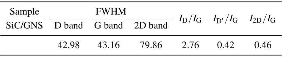
Table 1. Full widths at half maximum(FWHM)and relative intensity ratios of band-peaks of D, G, D′, and 2D (ID/IG, ID′/IG, and I2D/IG)for Raman spectra in Fig.3.
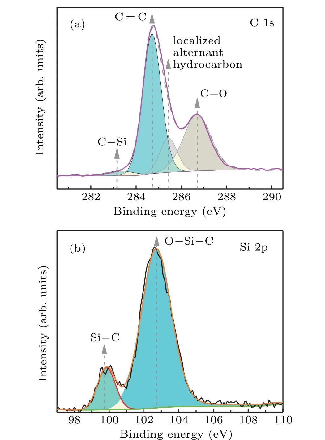
Fig.4. XPS spectra of SiC/GNS composites: (a)C 1s and(b)Si 2p.
To evaluate the quality of SiC/GNSs, XPS spectra of the SiC/graphene nanosheet film are shown in Fig. 4. As shown in Fig. 4(a), the C 1s spectrum contains four peaks at 283.1 eV, 284.7 eV, 285.4 eV, and 286.7 eV, which correspond to C-Si bond,[38]graphite C=C species,[39]localized alternate hydrocarbon,[30,40]and C-O bond.[41]In Fig. 4(b),two peaks related to Si-C (99.8 eV)[38,42]bond and O-Si-C(102.7 eV)[43]exist in the Si(2p)spectrum of SiC/GNS.Oxygen may come from physically adsorbed oxygen or oxygenrelated contamination.
3.2. Growth mechanism
The ionization rate of HWP is high, the TMS can be treated as fully ionized,and a large number of active free radicals exist inside the plasma. After a complex gas-phase reaction and a short-chain reaction,[44]SiH, CH, and C2 radicals are viewed as the primary species for SiC/GNS growth.[45]The loss of TMS methyl groups and the extraction of hydrogen are important nucleation approach and growth pathway.[20]The TMS reactions can be described by the equations in Ref.[46].

Fig.5. Illustration of initial growth model of SiC/GNS synthesized on Si substrate;[(a)-(d)]SEM images of SiC/GNS composites deposited at different times.
The initial growth mechanism model is given as follows.(i)Carbon-containing active radicals are adsorbed onto the Si substrate, and thus forming a very thin carbon layer. (ii) Silicon and carbon combine and fuse to form a sphere with a size of approximately 230 nm. The SiC nanocrystalline islands completely cover the substrate surface,and thus forming a rough surface interface layer with many dangling bonds on the substrate. These dangling bonds are the nucleation sites for graphene nanocrystals. (iii)Disordered carbon nanosheets nucleate there and undergo two-dimensional growth to form nanographene sheets. The formation mechanism of SiC/GNSs in the Ar/TMS HWP is the polymerization of neutral TMS fragments. Figure 5 describes the above-mentioned morphological evolution of SiC/GNSs surface.
High magnification SEM images of SiC/GNSs with different deposition times to observe its growth process are shown in Figs. 5(a)-5(d). Those results show that nanoislands of silicon and carbon initially nucleate during the initial nanosheet composite growth phase, an interface layer is constructed by aggregating the formed silicon and carbon nanoislands, and carbon nanosheets then grow at the nuclei on the interface layer. This is because the SiC nanoparticles agglomerate significantly,[47-49]which is consistent with a previous mechanistic model of SiC/GNS growth.
3.3. Electron temperature
Optical emission spectroscopy is used to diagnose HWP discharge,and shown Fig.6. An Hαline is found at 656.2 nm,meanwhile weak lines for Si(at 288.1 nm and 390.5 nm)and C(at 516.0 nm and 588.6 nm)species are also recorded. The lines for Si are found at 288.04 nm and 388.22 nm, which originate from the dissociation of the TMS. We can deduce the formation process of active species as follows: ((CH)3)4Si+ e-→SiH, Si, C2, H. Inert gases such as argon, neon and helium each play an important role in controlling electron temperature through excitation and ionization.[50]In a local thermal equilibrium(LTE)plasma,the electron temperature is the same as the excitation temperature,so the most common electron temperature can be calculated by the light intensity ratio method.[51]In order to understand the HWP discharge mode,we choose the two spectral lines 738.3 nm and 801.44 nm to calculate the electron excitation temperature. The electron temperatures are determined to be 1.7435 eV.
3.4. Photoluminescence
In addition,the fluorescence characteristics of SiC/GNSs on different substrates are also studied. Figure 6 shows the fluorescence spectrum of the SiC/GNSs synthesized at room temperature at 380 nm. Two strong fluorescence peaks are observed at 420 nm and 440 nm, the corresponding energies are about 2.95 eV and 2.82 eV (1240/wavelength = eV),[52]respectively. A single PL peak of graphene oxide can be observed in Ref.[53]. Our SiC/GNS sample generates multi-PL peaks, which indicate that the PL mechanism of SiC/GNS is complicated. The strong D peaks in Fig.3 and the large value ofID/IGindicate that the sample contains the definite sp3carbon and defects.[54]Thus,a bandgap is formed in the sample.The results of Fanchiniet al.[55]indicate that the energy difference betweenπ*state andπstate is~2.5 eV-3.5 eV although the optical gap is lower than 1 eV for carbon materials.Thus, the PL peaks centered at about 420 nm and 44 nm can be attributed to the transition between theπ*andπbands.[56]The PL results of films deposited on the quartz and silicon substrates show that their peak positions remain unchanged.Therefore,the substrate is not necessarily related to the PL performance of the material. The luminescence mechanism may be related to the quantum size effect of the nanomaterial.[57]These strong peaks are caused by material morphology,orientation,defects,and dangling bond surfaces.
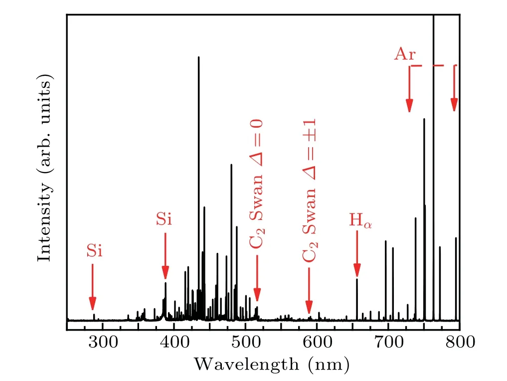
Fig.6. Optical emission spectra for Ar+TMS in HWP during synthesis of samples.
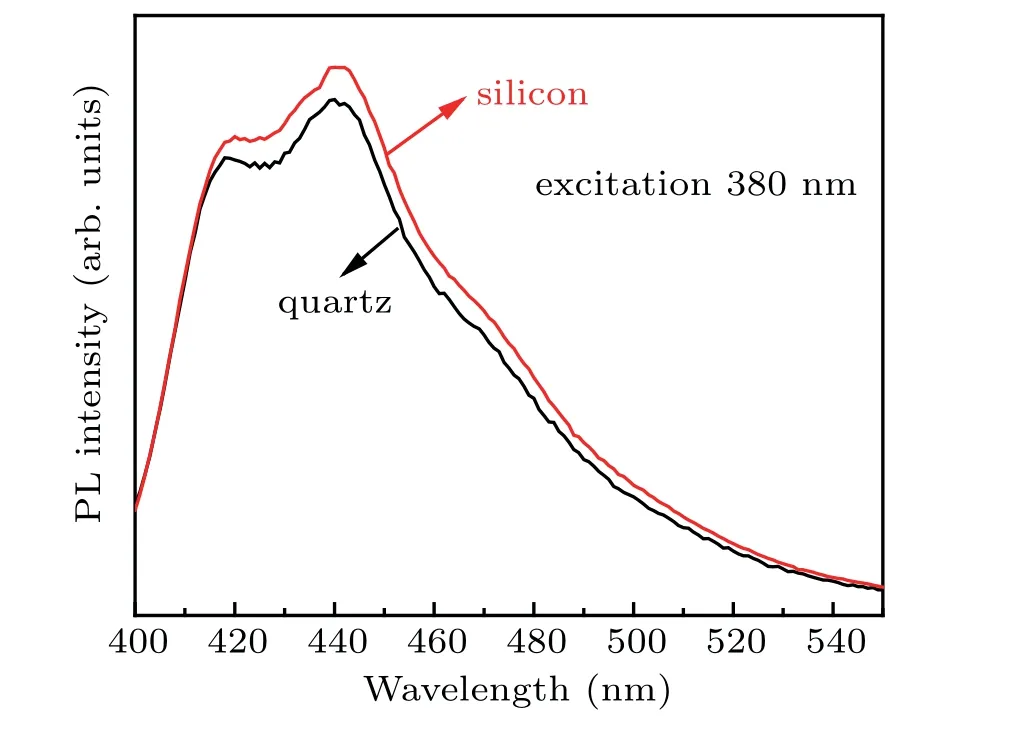
Fig. 7. PL spectra of SiC/GNSs on different substrates under excitation of 380-nm laser.
Compared with the bandgap of bulk 3C-SiC (2.23 eV),SiC nanowires (2.07 eV-2.48 eV)[58]and SiC nanoparticles(2.38 eV-3.10 eV),[59]the PL peak of SiC/GNSs (2.95 eV)is blue-shifted. Those results indicate that SiC/GNSs have the potential applications in serving as light-emitting materials with excellent thermal and oxidation stabilities. Therefore,the synthesis of SiC/GNSs should have broad applications in blue and ultraviolet light emission,field electron emission,and display devices.
4. Conclusions
In this study, SiC/GNSs composites are directly and rapidly synthesized by decomposition of TMS at low pressure,high density HWP discharge of Ar flow. Raman spectrum confirms the graphene structure. In the XRD and XPS studies, theα-SiC andβ-SiC are obtained on the surface of the SiC/GNS composite. Moreover, a diffusion-nucleation process describes nanosheet formation. Graphene nanosheets nucleate on many dangling bonds of the SiC nano-islands, then undergo two-dimensional growth, ultimately resulting in the formation of SiC/GNS composites. The electron excitation temperature is calculated to be about 1.7435 eV for the Ar+ TMS in the HWP during synthesis of samples. Comparing with other SiC, the PL peak of SiC/GNSs (2.95 eV) is blue-shifted, indicating that SiC/GNSs have the potential applications in serving as light-emitting materials with excellent thermal and oxidation stabilities.
Therefore,we expect these SiC/GNS composites to have broad applications in blue and ultraviolet light emission,field electron emission,and display devices.
猜你喜歡
Journal of Donghua University(English Edition)(2022年3期)2022-08-08 06:10:46
中學(xué)生博覽(2021年11期)2021-07-15 22:45:22
中學(xué)生博覽(2021年13期)2021-07-14 01:24:29
小讀者(2021年4期)2021-06-11 05:42:26
中學(xué)生博覽(2021年3期)2021-03-08 02:25:51
中學(xué)生博覽(2021年1期)2021-03-04 19:49:14
小哥白尼(軍事科學(xué))(2019年3期)2019-06-26 00:49:54
中學(xué)課程輔導(dǎo)·教學(xué)研究(2017年11期)2017-09-23 12:22:39
西部皮革(2015年17期)2015-02-28 18:14:55
作文周刊·小學(xué)一年級(jí)版(2014年43期)2014-05-30 10:48:04

- Chinese Physics B的其它文章
- Numerical simulations of partial elements excitation for hemispherical high-intensity focused ultrasound phased transducer*
- Magnetic-resonance image segmentation based on improved variable weight multi-resolution Markov random field in undecimated complex wavelet domain*
- Structure-based simulations complemented by conventional all-atom simulations to provide new insights into the folding dynamics of human telomeric G-quadruplex*
- Dual-wavelength ultraviolet photodetector based on vertical(Al,Ga)N nanowires and graphene*
- Phase-and spin-dependent manipulation of leakage of Majorana mode into double quantum dot*
- Deep-ultraviolet and visible dual-band photodetectors by integrating Chlorin e6 with Ga2O3