
High performance infrared detectors compatible with CMOS-circuit process*
2021-05-24 02:22:56ChaoWang王超NingLi李寧NingDai戴寧WangZhouShi石旺舟GuJinHu胡古今andHeZhu朱賀
Chinese Physics B 2021年5期
Chao Wang(王超), Ning Li(李寧), Ning Dai(戴寧),3,4,?,Wang-Zhou Shi(石旺舟), Gu-Jin Hu(胡古今),?, and He Zhu(朱賀)
1State Key Laboratory of Infrared Physics,Shanghai Institute of Technical Physics,Chinese Academy of Sciences,Shanghai 200083,China
2University of Chinese Academy of Sciences,Beijing 100049,China
3College of Physics and Optoelectronic Engineering,Hangzhou Institute for Advanced Study,University of Chinese Academy of Sciences,Hangzhou 310024,China
4Jiangsu Collaborative Innovation Center of Photovolatic Science and Engineering,Changzhou 213164,China
5Department of Physics,College of Mathematics and Science,Shanghai Normal University,Shanghai 200234,China
6Hangzhou Dianzi University,Hangzhou 310018,China
Keywords: Si:P,long wavelength detectors,blocked impurity band,terahertz
1. Introduction
Electromagnetic waves in a wavelength range of ~1μm–300 μm are widely used in infrared imaging, security inspection,earth observation,infrared astrophysics,extraterrestrial life science, and other fields.[1–5]A variety of detection technologies have been developed in order to meet various demands.[6–8]Generally speaking, infrared and terahertz detectors working in this frequency range can be divided into photoelectric devices and thermoelectric devices according to their working principles.[9]
The response speeds of the photoelectric devices are very fast, specifically, in a nanosecond range, while those of the thermoelectric devices are very slow, in a millisecond range.In the processing technology, photoelectric-based detectors are relatively complex due to the requirements for special materials and device structures.
Recent years,the so-called photoconductive blocked impurity band (BIB) infrared detectors have attracted much attention again due to their outstanding merits such as low dark currents, large photoconductivity gains, high resistance to irradiation, etc.[10–13]Petroff and Michael first proposed and demonstrated this type of device and established the basic model of responsivity and noise of the BIB detector.[14]For the silicon-based BIB device, the photoelectric response wavelength is mainly determined by the ionization energy of the doped atoms in the active layer. By introducing different impurities, peak wavelength can be tuned from 2.3 μm to 31 μm.[10,11,13]Most of the existing siliconbased BIB photoelectric detectors are fabricated by molecular beam epitaxy and standard Si process,which are expensive in cost.[5,10,11,13,15–20]Ion-implantation is a relatively-simple,highly-efficient,and cheap semiconductor-processing technology. It was first used to fabricate BIB detectors by Beeman et al. in 2007.[21]Illuminated by their ideas, we investigate a kind of planar configuration of Si-based photoconductive BIB detectors that are fabricated by using a modified Si-based process. With a DC bias voltage of ?2.3 V the normalized peak detectivity (D*) is as high as 4.9×1013cm·Hz1/2/W, and the responsivity is nearly 4.58 A/W.Both parameters are comparable to or even superior to the corresponding results reported in the literature.[5,10–12,16,19,21]Very importantly,the manufacturing method used for the present Si:P BIB detectors is almost compatible with that for the CMOS-circuit, thus significantly reducing the fabrication cost.
2. Experimental procedure
The device structure used here is similar to that described in Refs. [10–12,16]. Figure 1 shows the schematic diagram of device structure and the process flow chart of a Si:P photoconductive BIB detector. As shown in Fig. 1, the detector consists of two Al contact regions, a P-doped Si absorbing layer, an intrinsic Si blocking layer, and a passivation layer.The high-purity Si wafer,grown by the floating zone method,has a resistivity of 104?·cm.The two contact regions,respectively,with a P-atom density of 1020cm?3and 5×1017cm?3were achieved by P-ion implantation. In the direction of photocurrent transport,the widths of blocking layer and absorbing layer are 3μm and 50μm,respectively. The area of the photosensitive region is 50μm×1000μm. To ensure the uniform distribution of the P elements,multiple ion implantations were performed.The rapid thermal annealing at 950°C for 90 s was implemented to activate the P atoms and reduce the damage caused by ion-implantation. A layer of SiNxpassivating film with a thickness of 200 nm was deposited on a Si wafer surface by plasma-enhanced chemical vapor deposition. Owing to its compactness better than that of SiO2, SiNxis more effective for the passivation of Si surface. In addition,SiNxshows better performance in preventing atmospheric moisture from permeating into the device. Finally,a 600-nm-thick Al layer was prepared by using the electron beam evaporation,followed by reactive ion etching and lithographic patterning. A 30-min annealing treatment at 450°C was conducted for the deposited Al films to form Ohmic contact with the heavily-doped Si matrices.
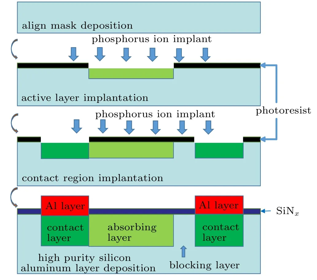
Fig.1. Schematic diagram of device structure and process flow chart of BIB detector.
The packaged detectors were mounted into a closed cycle cryogenic dewar equipped with a temperature controller. The photocurrent spectra were measured by a Nicolet 6700 Fourier transform infrared spectrometer,and the current–voltage(I–V)characteristic curves were recorded via a Kethily 236 semiconductor parameter analyzer. The blackbody response measurement system includes an 800-K blackbody source,a low-noise current amplifier (Stanford Research SR570), and a lock-in amplifier (Stanford Research SR830). The blackbody signal was chopped at a frequency of 277 Hz. Unless otherwise stated,all the photoelectric response measurements were performed at 5 K,and the infrared radiation was along the surface normal to the Si wafer.
3. Results and discussion
In a photoconductive BIB detector, the absorbing layer absorbs photons with very low energy, generating electron hole pairs. The electrons and holes are separated by using an applied voltage to drive photocurrent. The blocking layer is used to block the dark current. The performance of a BIB detector is mainly limited by its dark current(leakage current).The lower the leakage current,the higher the device detectivity is.Figure 2 displays the typical I–V characteristic curves of an ion-implanted Si:P BIB detector at several temperatures. It can be seen that the leakage current increases with temperature increasing. The reason is that with temperature increasing,more impurity states with shallow energy levels in Si material are thermally excited and release more electrons to conductive band, giving rise to a larger dark current at the same DC bias voltage. At 5 K, the I–V curve of the Si:P BIB detector shows a steep on-off character and the dark current is less than 0.05 nA in a bias voltage range from ?2.3 V to 2.3 V,revealing an important role of the blocking layer in inhibiting dark current. The breakdown voltage of the detector is about±2.4 V.Since a P atom has five valance electrons and acts as a donor in Si,the fabricated Si:P BIB detectors are all of n-type.For a BIB detector,the background impurity concentration Ndin the blocking layer is an important parameter determining the width of the depletion region and the tunneling current.Generally, the resistivity of the epitaxial Si blocking layer is about 10 ?·cm, corresponding to a doping concentration of 1014atom/cm3.[17]However, here in this work, the resistivity of the FZ-Si blocking layer reaches 20000 ?·cm at room temperature, Ndin the blocking layer is ~1012cm?3much lower than that in the epitaxial Si blocking layer and activating Si layer,resulting in a wider depletion region.On the other hand, in the blocking layer the average distance between two adjacent donor impurities is larger than 50 nm, the ionized+P cannot move freely and the impurity bands are interrupted.Thus, the detector leakage current is effectively reduced by the blocking layer. Additionally, according to semiconductor physics, a PN junction is termed electrical breakdown when the leakage current abruptly increase to one thousand times of its initial current value at a given reverse bias voltage. This voltage is called breakdown voltage. The breakdown mechanism of a PN junction generally includes avalanche breakdown, Zener breakdown, and thermal breakdown. Because the thickness of the blocking layer is about 3 μm, the width of the potential barrier in the depletion region is on the order of micrometer. Herein the breakdown of the Si:P BIB detector should be triggered by the avalanche breakdown.

Fig.2. Typical I–V characteristic curves of ion-implanted Si:P BIB detector at various temperatures.

Fig.3. Variation of detector responsivity with bias voltage at 5 K.
Figure 3 shows the responsivity for one of our Si:P BIB devices. The detector responsivity is measured by an 800-K blackbody source chopped at a frequency of 277 Hz. It can be found that the response photocurrent of the device increases slowly with the bias decreasing from 2.0 V to ?2.0 V.When the DC bias changes gradually from 2.0 V to the threshold voltage of ?2.4 V,the responsivity increases quickly and reaches a value of 4.58 A/W at ?2.3 V.At 5 K,the dark current of the detector is on the order of pA in a range of ?2.0 V to?2.3 V,so that the measured blackbody responsivity is dominantly contributed by photocurrent, indicating that the fabricated device has a very high photoelectric conversion efficiency.
The D*is an essential physical quantity characterizing the performance of a photoelectric detector,and expressed as[22]
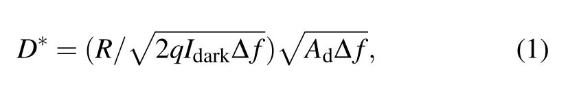
where R is the responsivity,Idarkis the dark current,Adis the area of the photosensitive element, q is the electron charge,and Δ f is the frequency band width of the current amplifier.
Figure 4 shows the calculated D*as a function of DC bias voltage for the Si:P BIB detector. The obtained D*value is as high as 4.9×1013cm·Hz1/2/W at a bias voltage of ?2.3 V,higher than those reported in Refs.[12,13,16,19]. We believe that both a small leakage current ~0.01 nA and a large responsivity ~4.58 A/W at 5 K and ?2.3 V bias are responsible for the high detectivity D*. For comparing, Table 1 lists the performance parameters of several kinds of BIB detectors.

Fig.4. Detectivity D* versus DC bias voltage of Si:P BIB detector at 5 K.

Table 1. Performance parameters of BIB detectors made by different methods.
In order to analyze the energy state of P impurities in the devices, photocurrent response in a mid-infrared-to-farinfrared range were measured by using the Nicolet 6700 Fourier transform infrared spectrometer with a solid substrate beam splitter and internal globar illumination. Figure 5 shows photocurrent response as a function of wavelength of the Si:P BIB detector biased at ?1 V.The response wavelength range of the device covers 2.5μm–35μm. The abrupt photocurrent decrease at ~16μm is due to the absorption of the transverse optical phonons and transverse acoustic phonons in silicon,while the response peat at ~31μm originates from the transition of P atoms from 1S state to 2P state.[19]

Fig.5. Spectral response versus wavelength of Si:P BIB detector biased at?1 V at 5 K.
The wavelength at the maximum photocurrent response,the peak responsivity, the full width at half maximum of the peak, and the cutoff wavelength toward the long-wavelength are ~27.3 μm, 80.1 A/W, 17.6 μm, and 29.5 μm, respectively. The photocurrent response of the Si:P BIB detectors in the wavelength range of 2.5μm–35μm stems from the P atom electron transition caused by the irradiation excitation.[19,23]
4. Summary
In summary, based on multiple ion-implantation and rapid thermal annealing treatment,a modified process is developed to fabricate high performance Si-based blocked impurity band detectors,and a significant reduction in production cost is realized due to a high compatibility of this process technology with CMOS-circuit. Compared with previously reported detectors, the fabricated photoconductive devices display comparable or even better to photoelectric response characteristics. At 5 K and a DC bias voltage of ?2.3 V,the responsivity and the detectivity of our best detector to the 800-K blackbody radiation are over 4.0 A/W and 4.5×1013cm·Hz1/2/W,which bring light to their potential applications of infrared astrophysics,infrared detection,and extraterrestrial life science.
- Chinese Physics B的其它文章
- Process modeling gas atomization of close-coupled ring-hole nozzle for 316L stainless steel powder production*
- A 532 nm molecular iodine optical frequency standard based on modulation transfer spectroscopy*
- High-throughput identification of one-dimensional atomic wires and first principles calculations of their electronic states*
- Effect of tellurium(Te4+)irradiation on microstructure and associated irradiation-induced hardening*
- Effect of helium concentration on irradiation damage of Fe-ion irradiated SIMP steel at 300 °C and 450 °C*
- Optical spectroscopy study of damage evolution in 6H-SiC by H+2 implantation*