
Preparation of AlN film grown on sputter-deposited and annealed AlN buffer layer via HVPE?
2021-03-19 03:21:58DiDiLi李迪迪JingJingChen陳晶晶XuJunSu蘇旭軍JunHuang黃俊MuTongNiu牛牧童JinTongXu許金通andKeXu徐科
Chinese Physics B 2021年3期
Di-Di Li(李迪迪), Jing-Jing Chen(陳晶晶), Xu-Jun Su(蘇旭軍), Jun Huang(黃俊),Mu-Tong Niu(牛牧童), Jin-Tong Xu(許金通), and Ke Xu(徐科),2,3,?
1Suzhou Institute of Nano-tech and Nano-bionics,Chinese Academy of Sciences,Suzhou 215123,China
2Suzhou Nanowin Science and Technology Co.,Ltd.,Suzhou 215123,China
3School of Physical Science and Technology,ShanghaiTech University,Shanghai 201210,China
4Key Laboratory of Infrared Imaging Materials and Detectors,Shanghai Institute of Technical Physics,Chinese Academy of Sciences,Shanghai 200083,China
Keywords: hydride vapor phase epitaxy(HVPE),AlN,threading dislocation(TD),sputter-deposition
1. Introduction
Recently, high quality AlN film has attracted a lot of interest due to its outstanding characteristics, like wide bandgap (6.2 eV), high surface acoustic wave velocity (5760 m/s in the c-plane), good thermal and chemical stability.[1,2]Especially, high quality AlN is crucial in fabricating deepultraviolet light-emitting diodes(DUV-LED)and laser diodes(LD), which play an important role in the field of water purification,medical treatment,and communication.[3]However,high threading dislocation density (TDD) of AlN would reduce the internal quantum efficiency (IQE) of DUV-LED.[4]In addition,pure screw threading dislocations would act as the leakage path in p-n diodes.[5]Therefore, it is significant to fabricate high quality AlN with low TDD for the application.
Homoepitaxy is considered as an ideal method to grow high quality AlN films with low TDD due to the same lattice constant and thermal expansion coefficient between the substrate and epilayer.[6,7]Nevertheless, the heteroepitaxy strategy is more widely used, ascribing to the lack of natural intrinsic substrates. As is well-known, the sapphire is the most commonly used substrates for fabricating AlN template due to its high UV-transparency and low cost. Many researchers have devoted tremendous effort to improve the quality of AlN film on sapphire substrates, such as the multi-step growth[8-10]and epitaxial lateral overgrowth on patterned sapphire substrates.[11,12]However, TDDs of the AlN films are still among the order of 109-1010cm?2, due to the poor Al adatom mobility.[13]Miyake et al. proposed that overlapped“face-to-face” high-temperature (HT) annealing could suppress the thermal decomposition of the AlN films, which is effective in reducing the TDD.[14]They have succeeded in fabricating high quality AlN by combing MOVPE with a sputterdeposited annealed AlN buffer layer. However, there are few reports about growing AlN films on sputter-deposited and annealed AlN layer by hydride vapor phase epitaxy(HVPE).A detailed investigation of it is important for the stable growth of high-quality AlN films.
In this report, the AlN films were prepared on a sputterdeposited AlN buffer layer,which was annealed at a high temperature of 1500°C,with a home-built horizontal HVPE system. The dependence of the surface morphology,crystallinity,and microstructure of the HVPE-AlN layer on various growth V/III ratios was investigated,which would be beneficial for the growth of high-quality AlN films.
2. Experiments
25 nm-thick AlN layers were sputtered on 2-inch cplane sapphire substrates by sputtering technology. The radio frequency power and growth temperature were 750 W and 650?C,respectively. The AlN thick films with average thicknesses of about 5.5 μm were then grown on sputtered AlN buffer layers in a home-built HVPE system by the following procedures: initially, the 25 nm-thick sputtered AlN/sapphire was heated to 1500?C in flowing NH3, and then annealed in an H2and N2mixture atmosphere with a total chamber pressure of 20 hPa for 30 min. After that, a 5.5 μm-thick AlN film was grown on sputter-deposited annealed AlN/sapphire by HVPE.In the experiments,the reactor chamber was maintained at 10 hPa, the AlCl3and N2flow rates were 50 and 200 sccm, respectively, and the carrier H2flow rates were 2000 sccm. AlCl3was generated in the reactor(source zone)by the reaction between Al metal and HCl gas at 500?C. In this work,three samples grown with different V/III ratios were compared,and their growth conditions were shown in Table 1.The V/III ratio,namely,the N2/AlCl3ratio,was calculated by the input flux ratio of N2and HCl gas,assuming that HCl fully reacted with metal Al to form AlCl3.
High-resolution x-ray diffraction (Bruker D8 Discover,EUR)was used to characterize the crystal quality of the AlN films. Atomic force microscopy (Veeco Dimension ICON,USA) was applied to measure the surface morphology of the AlN films in tapping mode. The microstructure observations were performed on a transmission electron microscope (TALOS F200X, USA) with an accelerating voltage of 200 kV.The cross-sectional specimens for TEM measurements were prepared by mechanical polishing and followed by the Ar+ion milling process.
Table 1. Growth conditions of as-grown AlN samples,as well as the full width at half-maximum(FWHM)value of(0002)and(10ˉ12)plane x-ray rocking curves(XRCs)for HVPE-AlN films.
3. Results and discussion
To evaluate the crystalline quality of as-fabricated AlN samples with different V/III ratios, the x-ray rocking curves(XRCs) of the symmetric (0002) and asymmetric (10ˉ12)diffractions for three AlN samples from A to C were conducted,respectively,with the corresponding full width at halfmaximum (FWHM) values derived, as shown in Fig.1. The following equations can be used to further estimate the density of screw and edge dislocations for AlN samples:[15,16]
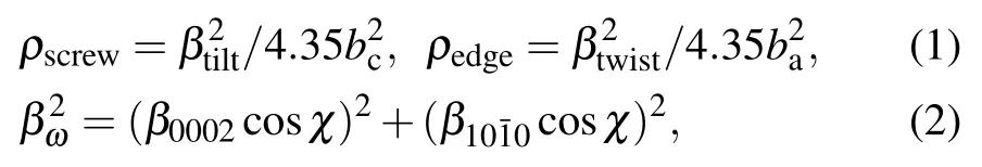
where βtiltand βtwistare the tilt and twist angle of(0002)and(10ˉ10) planes and are expressed in radian; bcand baare the burgers vectors of c-type and a-type threading dislocations,respectively;β10ˉ10can be calculated by Eq.(2)and χ is the angle between(10ˉ12)plane and the normal line of(0001)basal plane.
As shown in Fig.1(c),the FWHM values of(0002)plane for samples A-C are 294, 64, and 165 arcsec, corresponding to the density of screw TD of about 1.9×108,8.9×106,and 5.9×107cm?2, respectively. Meanwhile, the FWHM values of (10ˉ12) plane for samples A-C are 652, 648, and 682 arcsec,corresponding to a density of edge TD of about 4.6×109,5.1×109, and 5.5×109cm?2, respectively. It suggests that sample B,with the growth V/III ratio of 150,has the narrowest FWHMs, namely the best crystalline quality. Figure 1(d)shows the orientation of the sputtered AlN buffer layer before high-temperature annealing. It can be found that the (0002)and(0004)peaks of AlN and(0006)peaks of Al2O3are obvious,indicating the high c-axis orientation of the sputtered-AlN buffer layer.
Figure 2 presents the AFM images of AlN samples from A to C, respectively, to reveal the morphology evolution of samples with V/III ratios increasing. The insets are the magnified AFM images. As shown by Fig.2(a),sample A grown at a V/III ratio of 100 shows uncoalesced hexagonal islands on the surface. When the V/III ratio is higher than 150, AlN films show hillock-like surface structure,as seen in Figs.2(b)and 2(c). This can be attributed to the low density of screw TD and mixed TD with screw-component,since the high density screw and mixed TD would impede the lateral enlargement of spiral growth, and thus the hillocks form on the AlN surface.[17,18]According to the previous XRD results, sample B has the narrowest FWHM of(0002)plane,which means the smallest density of screw TD. Namely, sample B has the smallest spiral growth resistance, which would facilitate the formation of the hillock structure, while the opposite case is true in sample A. In addition, the root mean square (RMS)values of surface roughness for samples (see the insets) are 4.69, 0.75, and 0.20 nm, respectively. Obviously, the surface roughness of the HVPE-AlN decreases when the V/III ratio of the regrowth increases.
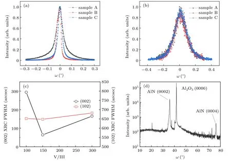
Fig.1. XRD rocking curves of(a)AlN(0002)plane and(b)plane for AlN samples with different V/III ratios,(c)FWHMs of(0002)plane andplane for AlN samples based on(a)and(b),respectively. (d)The full XRD pattern of the 25 nm thick sputtered-AlN buffer layer before high-temperature annealing.
Fig.2. AFM images of the HVPE-AlN films grown on sputter-deposited and annealed AlN buffer layer: (a) sample A, (b) sample B, and(c)sample C.The insets present the magnified AFM images of the samples, correspondingly. The scale bars are 2μm, while 400 nm in the inset. The height of morphology is indicated by color scales at the right side of each image,where 50,5,and 5 nm are the maximum value of the color scales.

To improve the TDs imaging quality, the typical high magnification WBDF images of the AlN/sapphire interface are presented in Fig.4. As illustrated by Fig.4, the edge TDs near the AlN/sapphire interface in the AlN samples have different propagation behavior. Specifically, edge TDs in samples A and B bend slightly in the first 400 nm region above AlN/sapphire interface (see Figs. 4(a) and 4(b)). However,the TDs in sample C are mostly vertical to the (0001) basal plane (see Fig.4(c)). Compared with sample C, TDs stand a better chance to interact with each other in samples A and B before propagating to the surface. This may explain the fact that the sample C with the highest V/III ratio has the highest TDD among the three samples,and the lower V/III ratio would improve the crystal quality.[20]
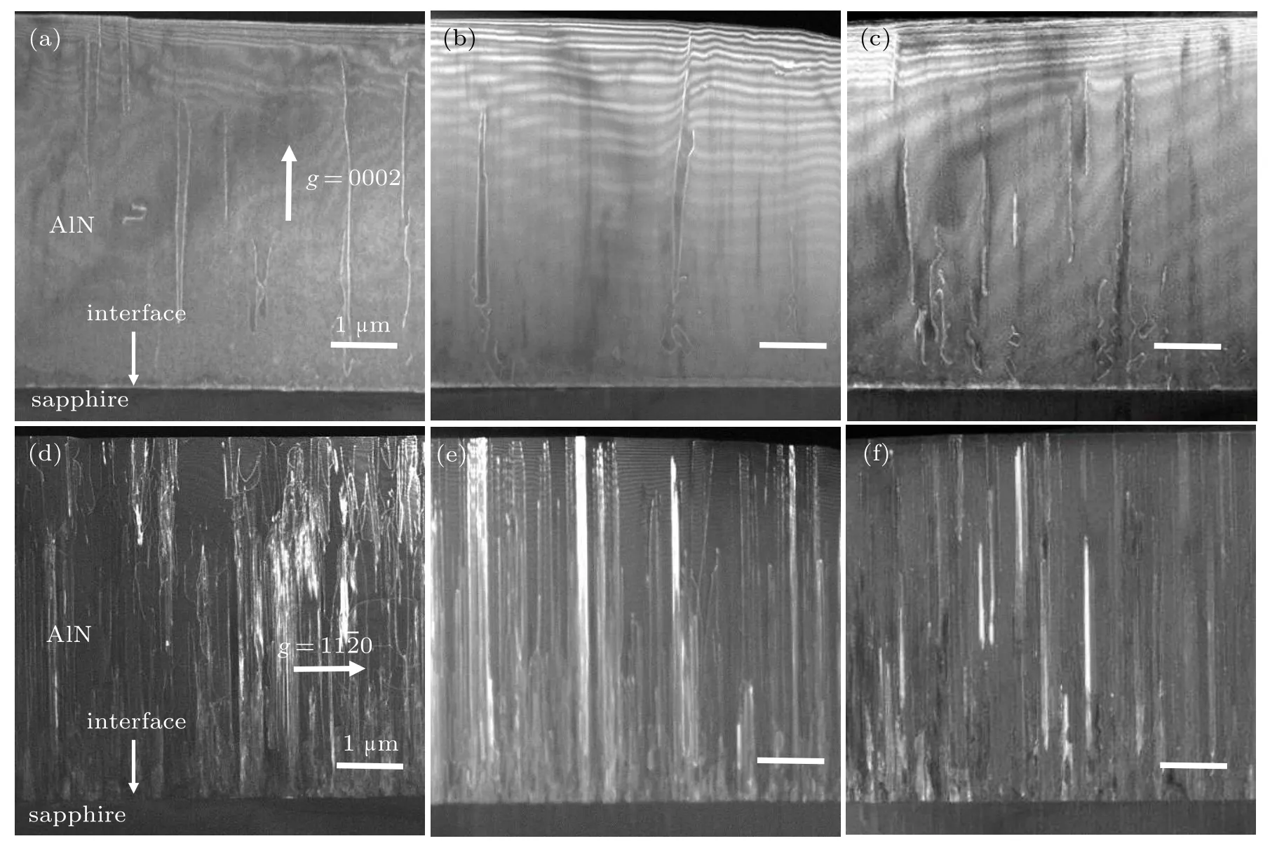
Fig.3.Cross-sectional weak beam dark field(WBDF)images under the two-beam condition:(a)and(d)for sample A,(b)and(e)for sample B,(c)and(f)for sample C.The upper row images are recorded with g vector of g=0002,and the lower row images are recorded with g=11ˉ20.The scale bars are 1μm.
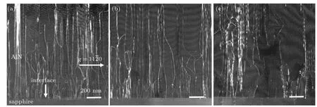
Fig.4. Weak beam dark field images (WBDF) of the AlN/sapphire interface: (a) for sample A,(b) for sample B,and (c) for sample C. The images are recorded with g vector of g=11ˉ20,and the scale bars are 200 nm.
The strain distribution near the HVPE-AlN/sputtered-AlN/sapphire interfaces for AlN samples has been analyzed by high resolution transmission electron microscopy (HRTEM)combined with geometric phase analysis(GPA),[21]based on the slight distortion of lattice fringes in HRTEM,as shown in Fig.5. Figures 5(a), 5(c)and 5(e)are the HRTEM images of HVPE-AlN/sputtered-AlN/sapphire interfaces for sample AC,respectively. In addition,the selected area electron diffraction (SAED) shows the orientation of the sputtered-AlN after high-temperature annealing (shown insets). The sputterdeposited and annealed AlN buffer layers are indicated by two black lines.
The thickness of the sputter-deposited annealed AlN buffer layer in Fig.5 is less than 25 nm, attributed to the decomposition of the AlN sputter layer during the high temperature annealing and growth. Simultaneously, the HVPEAlN/sputtered-AlN/sapphire interfaces become rough with voids of different sizes generating around them in samples.The nano-voids are speculated to be caused by the decomposition of sputtered-AlN[22]or sapphire (Al2O3)[23]during the high temperature annealing process. The decomposition of sapphire(Al2O3)at high temperature(above 1300?C)is a common phenomenon,and the decomposition is governed by the following chemical reaction:[24,25]Al2O3(s)+3H2(g)=2Al(g)+3H2O(g).

Fig.5. Cross-sectional high resolution transmission electron microscopy(HRTEM)images of HVPE-AlN/sputtered-AlN/sapphire interfaces(a)for sample A,(c)for sample B,and(e)for sample C;(b), (d)and(f)are the GPA images corresponding to the(a),(c)and(e), respectively, with the extracted strain data along the white dot lines in them on their right sides. The insets are the selected area electron diffraction patterns near the interface. The incident beam is along the[11ˉ20]zone axis and the scale bars are 20 nm.
4. Conclusion
In summary, AlN films grown on the sputter-deposited and annealed AlN buffer layer,by high-temperature(HVPE),have been fabricated at different V/III ratios.When the growth V/III ratio is 150, the crystalline quality of AlN films can be optimized in our experiments, and the XRC FWHM values of (0002)- and (10ˉ12)-planes are 64 and 648 arcsec, respectively. According to AFM observations, the higher growth V/III ratio would be beneficial to the hillock structure formation of AlN films, probably due to the low density of screw and mixed TDs. Otherwise, the uncoalesced islands structure would appear. The screw TDs in the as-grown AlN films obliquely form loops or half-loops after generation. Therefore,the TDs reaching to the surface of AlN films are mainly the edge TDs. Finally, after the high-temperature annealing,the HVPE-AlN/sputtered-AlN/sapphire interfaces get rougher and voids of different sizes generate around them. For the best crystalline quality sample,the voids are big enough to extend from sapphire to HVPE-AlN, which would be beneficial to relax the interface strain, and thus improving the crystalline quality of samples.
猜你喜歡
小學(xué)生學(xué)習(xí)指導(dǎo)(高年級(jí))(2023年3期)2023-03-31 06:03:22
紅蜻蜓·中年級(jí)(2022年11期)2022-11-23 08:53:00
瘋狂英語·新悅讀(2021年5期)2021-06-08 01:54:06
作文評(píng)點(diǎn)報(bào)·低幼版(2020年32期)2020-07-23 06:46:25
幽默大師(2020年5期)2020-06-22 08:19:26
青年生活(2019年3期)2019-09-10 16:57:14
作文小學(xué)中年級(jí)(2019年6期)2019-07-25 01:11:58
黃河之聲(2018年24期)2018-03-16 02:52:34
中國(guó)房地產(chǎn)業(yè)(2016年4期)2016-12-06 05:26:16
作文周刊·小學(xué)一年級(jí)版(2016年1期)2016-08-12 13:01:36

- Chinese Physics B的其它文章
- Nonlocal advantage of quantum coherence in a dephasing channel with memory?
- New DDSCR structure with high holding voltage for robust ESD applications?
- Nonlinear photoncurrent in transition metal dichalcogenide with warping term under illuminating of light?
- Modeling and analysis of car-following behavior considering backward-looking effect?
- DFT study of solvation of Li+/Na+in fluoroethylene carbonate/vinylene carbonate/ethylene sulfite solvents for lithium/sodium-based battery?
- Multi-layer structures including zigzag sculptured thin films for corrosion protection of AISI 304 stainless steel?