
Polymer/silica hybrid waveguide Y-branch power splitter with loss compensation based on NaYF4:Er3+,Yb3+nanocrystals?
2019-11-06 00:44:28YueWuFu符越吾TongHeSun孫潼鶴MeiLingZhang張美玲XuChengZhang張緒成FeiWang王菲andDaMingZhang張大明
Chinese Physics B 2019年10期
Yue-Wu Fu(符越吾),Tong-He Sun(孫潼鶴),Mei-Ling Zhang(張美玲),Xu-Cheng Zhang(張緒成), Fei Wang(王菲),?, and Da-Ming Zhang(張大明)
1State Key Laboratory of Integrated Optoelectronics,College of Electronic Science and Engineering,Jilin University,Changchun 130012,China
2College of Communication Engineering,Jilin University,Changchun 130012,China
Keywords:polymer,NaYF4:Er,Yb,loss compensation
1.Introduction
In recent years,optical communication technology has received a lot of attention and been rapidly developed due to its fast and effective transmission characterization.[1–3]While chasing the extraordinary performance in optical transmission,the functions of processing signal are also required,which makes many optical devices widely used.[4–6]Optical waveguide Y-branch power splitter,achieving the functionality of an optical power splitter,is one of the important devices in the integrated optical circuits. It can be used as a basic unit in the optical integrated devices,such as switches,couplers,and interferometer or easy integration with other separate optical devices such as lasers,modulators,and wavelength division multiplexers(WDM).It has important application prospects in terms of optical communication,sensors,energy distribution,etc.[7–11]
To seek a better performance of the Y-branch power splitter,many materials have been used as the core of the waveguide. Li et al.fabricated a single mode Si–Ge Y-branch at 1.55μm in 2002.[12]And in 2010,Jonathan et al.fabricated a lossless optical amplifier and Y-branch power splitter device in Al2O3:Er3+on silicon,which realized the ability to compensate for the loss in optical power splitter device.[13]Two years later,Chen et al.fabricated an Si-based photonic crystal waveguide Y-branch power splitter.The device has a good performance in the capability of good optical transmission and power-splitting.[14]Recently,the polymer waveguide has become a relevant research focus. Compared with traditional inorganic material,polymer material has advantages in easy processing and low transmission loss in the infrared band.The polymer waveguide is fabricated by using the traditional semiconductor technology,thus making it suitable for high density integrated optoelectronic devices.
With the development of the integrated photoelectronic device industry,higher integration has become a key element.Integrating more optical devices on a chip has been a major trend for a long period. In a highly integrated chip,the losses of individual devices will be superimposed on each other,which may cause a serious influence on the final quality of the photoelectronic chip.Therefore,optical amplifiers[15,16]and optical devices with loss compensation have become key components for photoelectronic device industry.[17–19]
Rare-earth (RE)-doped polymer, including erbium complex[20]and erbium-doped fluoride matrix nanoparticles,is widely used for fabricating optical waveguide amplifiers.Li et al.synthesized oleic acid(OA)-modified LaF3:Er,Yb nanoparticles,which could be used to synthesize the core material for the waveguide amplifiers.[21]Lei et al.synthesized OA-coated NaYF4:Er,Yb nanocrystals,which were doped into KMBR as the core material.The fabricated polymer waveguide amplifier with the above material achieved a relative gain of 4.7 dB/cm.[22]NaYF4is a fluoride matrix material with low phonon energy and high stability. Erbium and ytterbium co-doped NaYF4nanocrystals can generate photoluminescence around 1530 nm under 980-nm laser excitation,which has become a popular material for waveguide amplifiers and loss compensation devices.[23,24]In 2013,Zhai et al.synthesized NaYF4:Yb3+,Er3+,Ce3+-doped SU-8 2005 polymer waveguide amplifiers and reported a relative gain of 4.0 dB/cm.[25]Two years later,Yin et al.fabricated an optical waveguide amplifier based on erbium–ytterbium co-doped NaYF4nanocrystals doped into SU-8.The gain of the device was 3.42 dB/cm.[26]With NaYF4:Er,Yb nanocrystals,Xing et al.fabricated a polymer waveguide thermo-optical switch with loss compensation.The loss compensation of the device was 3.8 dB at 1530 nm.[18]
In view of the importance of optical devices with loss compensation in optical fiber communication,in this work we propose,design,and successfully fabricate a Y-branch power splitter device with loss compensation. To achieve a better performance of the Y-branch power splitter,SiO2is chosen as the bottom cladding of the device and therefore making it easy to integrate with other optoelectronic devices.The Y-branch with a structure of rectangular groove is fabricated by etching SiO2,and the core material is filled into the groove to obtain the complete waveguide structure.By this method,we realize a better waveguide topography,and the insertion loss is reduced effectively.First,NaYF4:Er3+,Yb3+nanocrystals are synthesized by using a high temperature thermal decomposition approach and their morphologies are characterized.We use Rsoft and COMSOL software to simulate the optical field of the device and the power distribution of the Y-branch power splitter.The characteristic parameters of the Y-branch are designed and optimized by using the simulated results. Then the nanocrystals are doped into SU-8 as the core material of the optical waveguide amplifier and spin-coated on the surface of the etched SiO2groove to realize a structure of embedded waveguide.Polymethyl methacrylate(PMMA)is used as the upper cladding.Throughout the fabrication,the traditional semiconductor technology such as spin-coating,photolithography,and development is used.Finally,the performance of the device is tested by the direct coupling.
2.Loss compensation principle
The loss compensation principle of Y-branch power splitter is based on optical amplification of the Er3+–Yb3+codoped system at 1530-nm wavelength under the 980-nm excitation.The energy level of Er3+–Yb3+co-doped system is shown in Fig.1.The Yb3+ion acts as a sensitizer in the energy level system.It shows a higher absorption cross section than Er3+ion and the concentration quenching does not occur under a high Yb3+doping concentration because it is a two-level energy system.The band gap between levels2F7/2and2F5/2of Yb3+ion equals that between levels4I15/2and4I11/2of Er3+ion.First,the ground-level2F7/2of Yb3+ions can efficiently absorb the pump energy at 980 nm and transit up to the excitation-level2F5/2,then transfer the energy to the level4I15/2of Er3+ions to help them transit up to the unsteady excitation-level4I11/2.After they decay to the metastable level4I13/2,the population inversion between excitation level and the ground level is obtained. Then the stimulation emission starts,generating light around 1530 nm that is the same as the signal wavelength. Therefore,the amplification function for the signal light is finally realized.
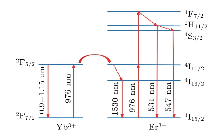
Fig.1.Energy levels of Er3+–Yb3+co-doped system.
3.Experiment
3.1.Waveguide material preparation
In this work,NaYF4:Er3+,Yb3+nanocrystals were synthesized by using a high temperature thermal decomposition approach.RECl3·6H2O(2 mmol),including YCl3·6H2O(1.6 mmol), ErCl3·6H2O(0.04 mmol), and YbCl3·6H2O(0.36 mmol),was added into a three-necked flask.Octadecene(30 mL)and OA(12 mL)were poured into the same flask.The mixture was heated to 100?C for 10 min and then raised to 150?C and heated for 30 min.With a flow of argon as the protective gas,the solution in the flask was cooled to room temperature. Meanwhile,two solutions of NH4F(8 mmol)dissolved in methanol(20 mL)and NaOH(5 mmol)dissolved in methanol(10 mL)were added dropwise into the flask.To evaporate the methanol,the flask was kept at 50?C with continuously stirring for 1 h. Then the solution was heated at a constant temperature of 310?C for 1 h under the protective gas argon and finally cooled to room temperature naturally. After the reaction,the nanocrystals were collected by repeatedly washing with ethanol and centrifugation.The synthesized nanocrystals were modified by OA and they are soluble in toluene.High-concentration Er3+is conducive to enhancing the gain of device,but the high doping concentration of nanocrystals in polymer matrix will cause the nanoparticles to be aggregated,thus producing a large scattering loss.In our experiments,nanocrystals(0.3 mmol)were dissolved in the toluene(2 mL)and the solution was mixed into SU-8 2002. After being agitated ultrasonically for 2 h,nanocrystals with OA-modified surface were uniformly dispersed in the SU-8 2002,and the core material with 0.4 wt%concentration of nanocrystals in polymer was obtained.
3.2.Characterization
The NaYF4:Er3+,Yb3+nanocrystals were characterized in terms of their morphology and emission properties. The sizes of the samples were characterized by a transmission electron microscopy(TEM:JEOL JSM-7500F).Figures 2(a)and 2(b)show the TEM image of the nanocrystals and the histogram of size distribution.The particle sizes of the nanocrystals prepared by this method ranged from 6 nm–11 nm with a mean diameter of 8 nm.The core material was spin-coated with a thickness of 1μm on the surface of silicon chip to test its film-formation.The atomic force microscopy(AFM)micrograph of the core material film with a square mean roughness value of 0.407 nm and maximum surface fluctuation of 2.8 nm is shown in Fig.3,demonstrating that the nanocrystals were well dispersed into SU-8 without particle aggregation and thus the surface of the film was smooth. The absorption spectrum and emission spectrum pumped by a 980-nm laser of the nanocrystals were obtained.The full width at half maximum of the emission was about 83 nm.The absorption spectrum and the emission spectrum are shown in Figs.4(a)and 4(b),respectively.

Fig.2.(a)The TEM image of NaYF4:Er3+,Yb3+nanocrystals(b)histogram of particle size distribution.
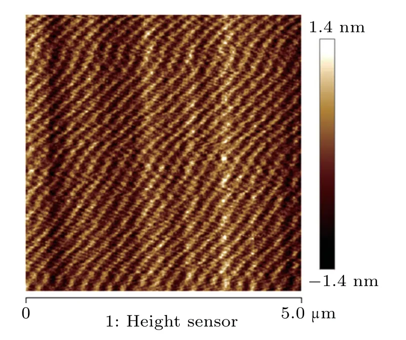
Fig.3.The AFM image of core film.
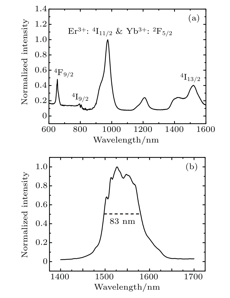
Fig.4.(a)Absorption spectrum of nanocrystals and(b)emission spectrum of nanocrystals with excitation of 980-nm laser.
3.3.Analysis and simulation
The structure of the waveguide Y-branch power splitter was designed based on the cosine curve. Figure 5(a)shows that the specific structure of the device consists of an input waveguide,two transition waveguides,and two output waveguides.The function expression of the cosine curve waveguide is
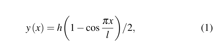
where l is the length of the transition zone,h is half of the distance between two branches,and the zero point of the coordinate axis is the starting point of the branch.When x=l,the transition of Y-branch ends.The above parameters were marked in Fig.5(b). Based on the simulation and experiment,the parameter values of the structure were chosen as l=4000μm and h=50μm.
The two branches have the same optical properties,including the same material,structure,and waveguide width.When the signal light reaches the branch point,the power will be evenly output into the two branches,making the Y-branch a 3-dB power splitter.
As shown in Fig.6(a),the embedded waveguide structure with etched SiO2was used as the bottom cladding,nanocrystal-doped SU-8 as the core,and PMMA as the upper cladding. The refractive index of the bottom cladding,core and upper cladding were measured to be 1.46,1.57,and 1.48 at 1530 nm,respectively.Taking into account the precision of the fabrication process,simplicity of testing,and characteristics of the core and cladding material,w=6μm was chosen as the waveguide width and b=6.5μm as the total core thickness with the groove height a=5.5μm.The optical field distribution of the waveguide at 1530 nm was simulated by COMSOL,and the light was well confined within the core region with a power confinement of 92.6%as shown in Fig.6(b).
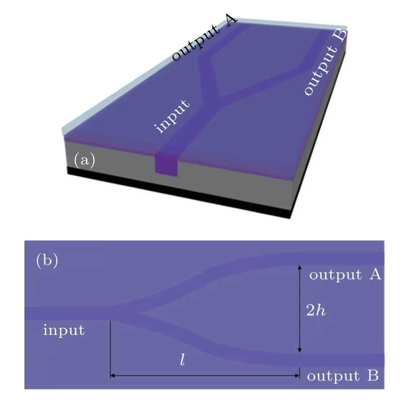
Fig.5.(a)Schematic diagram and(b)top view of device.
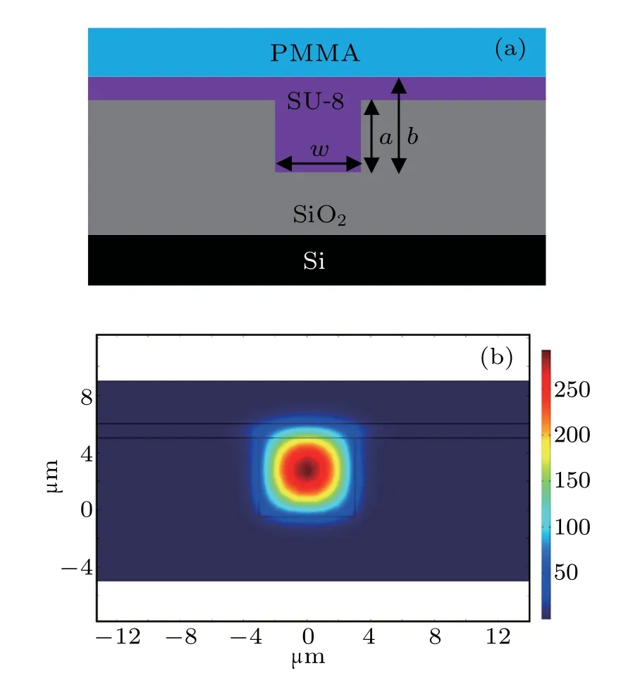
Fig.6.(a)Schematic diagram of cross-section and(b)simulated optical field distribution in waveguide.
The optical power distribution of the waveguide under the transverse magnetic(TM)polarization was simulated by Rsoft. Figures 7(a)and 7(b)show the simulation results of optical power distribution at 1530 nm and 980 nm.The green lines in the figures represent the change of optical transmission power in the Y-branch power splitter.After passing through the branch point,the output power of each branch was only half of the input power,thus realizing the function of a 3-dB power splitter.
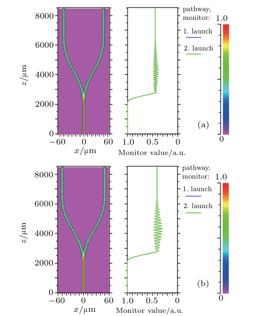
Fig.7.Rsoft simulated optical power distribution of TM waveguide mode at(a)1530 nm and(b)980 nm.The unit a.u.is short for arbitrary units.
3.4.Fabrication
High-concentration nanocrystals doped in SU-8 will cause the breakage on the waveguide during photolithography and development. Therefore,we used an embedded waveguide structure to overcome this difficulty. By etching the SiO2,we obtained the rectangular grooves with the shape of Y-branch.Then the nanocrystals-doped SU-8 was spin-coated to fill the groove.Finally,PMMA was spin-coated as the upper cladding of the device.
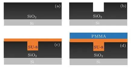
Fig.8.Preparation process of Y-branch power splitter.
Figure 8 shows the process of preparation of the Y-branch power splitter. Both the easy integration and low fabrication cost will be obtained by this method.Figure 9(a)shows the scanning electron microscopy(SEM)image of the groove cross-section on the SiO2substrate embedding no core material. And figure 9(b)exhibits the SEM micrograph of the cross-section of the waveguide embedding the core material without the upper cladding.
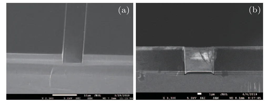
Fig.9.The SEM image of(a)groove on the SiO2 substrate and(b)crosssection of waveguide without upper cladding.
3.5.Testing
First,we cleaved both input cross-section and output cross-section of the Y-branch power splitter. Each port of the device was separately coupled to the optical fiber by direct coupling.Figure 10 shows the schematic diagram of the test system of optical loss compensation measurement.A tunable laser(Santec TSL-210)with a wavelength range from 1510 nm to 1590 nm and a 980-nm laser were used as the signal source and pump source respectively.The signal light and pump light were coupled by a WDM to launch into the input cross-section of Y-branch power splitter.The output light from the cross-section of the device was collected and coupled into a spectrum analyzer(OSA,ANDO AQ-6315 A).Finally,we observed the two branches of the Y-branch power splitter separately to analyze the loss compensation characteristics of the device.

Fig.10.Structural diagram of test system.
The relative gain of the device was calculated from the following formula:

The test results are shown as follows.Figure 11(a)shows the output pattern of the device with 1530-nm signal light.The input signal light was evenly distributed across the two branches after passing through the Y-branch,thus obtaining two output spots.Figure 11(b)shows the upconversion luminescence of the Y-branch power splitter. The up-conversion green light occurred under the excitation of 980-nm pump laser and the light path was clear and uniform,demonstrating that the nanocrystals were uniformly dispersed in the core material.
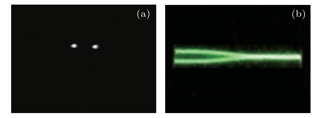
Fig.11.(a)Output pattern of device,(b)Y-branch power splitter with upconversion luminescence under excitation at 980 nm.
Each of branches was tested separately.When the signal light power was 1 mW,the insertion losses of two branches were ?14.8 dB and ?15.1 dB at 1530 nm,respectively.Figures 12(a)and 12(b)show the relative gain versus pump power for 1530-nm signal light,respectively of branch A and branch B.For the input signal power of 0.05 mW and the pump power of 267.7 mW,the loss compensation of two branches were 5.81 dB and 5.41 dB,respectively.And when the signal light power was 1 mW,the relative gains were 1.73 dB and 1.72 dB.Comparing within different signal power,it can be found that the loss compensation for small signal is better than for large signal.Figures 12(c)and 12(d)show the relationship between relative gain and pump power with a signal power of 0.05 mW,relatively,of branch A and branch B.The relative gain are 3.5 dB and 2.95 dB,respectively,at 1540 nm and 1550 nm.The maximum relative gain is 5.81 dB at a wavelength of 1530 nm.The insertion loss and relative gain of the two branches are almost the same,which proves that the basic function and loss compensation function of the Y branch are well achieved.The above test results of the device at different signal wavelengths are consistent with the emission characteristics of the nanocrystals.
In this work,we doped the NaYF4:Er,Yb nanocrystals into SU-8 as amplification material.Rare-earth nanocrystals can be doped in many polymer materials by different methods.Polymethyl methacrylate(PMMA)is a common polymer and the main component of polymer fiber.Compared with doping nanocrystals into the polymer,nanoparticles-PMMA covalentlinking is a good method in terms of reducing the aggregation of nanocrystals and increasing the nanocrystals doping concentration in polymer matric.Optical waveguide devices with loss compensation will play an important role in photonic integration on chip.
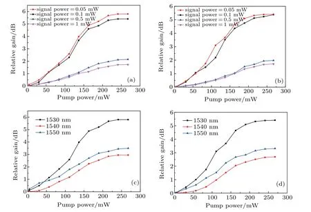
Fig.12.Relative gain at 1530-nm wavelength versus pump power for different signal powers of(a)branch A and(b)branch B.Relative gain versus pump power for signal power of 0.05 mW at different signal wavelengths of(c)branch A and(d)branch B.
4.Conclusions
In this work,a polymer waveguide Y-branch power splitter with loss compensation based on NaYF4:Er3+, Yb3+nanocrystals is proposed and investigated. During the fabrication of the device,SiO2is used as the bottom cladding,nanocrystal-doped SU-8 as the core material,and PMMA as the upper cladding.The whole device is designed with a structure of embedded waveguide.The fabricated device realizes the functions of power splitting and loss compensation.The insertion loss for each of the two branches of the Y-branch power splitter is about 15 dB.When the 980-nm pump power is 0.05 mW and the signal power is 267.7 mW,the maximum relative gain of a single branch is 5.81 dB at 1530 nm.The proposed Y-branch power splitter with loss compensation can improve the stability of optical device and therefore has a great research significance.

- Chinese Physics B的其它文章
- Theoretical analyses of stock correlations affected by subprime crisis and total assets:Network properties and corresponding physical mechanisms?
- Influence of matrigel on the shape and dynamics of cancer cells
- Benefit community promotes evolution of cooperation in prisoners’dilemma game?
- Theory and method of dual-energy x-ray grating phase-contrast imaging?
- Quantitative heterogeneity and subgroup classification based on motility of breast cancer cells?
- Designing of spin filter devices based on zigzag zinc oxide nanoribbon modified by edge defect?