
A 5.4mW and 6.1% efficiency fixed-tuned 214GHz frequency doubler with Schottky barrier diodes*
2015-02-15 02:19:20YaoChangfei姚常飛ZhouMingLuoYunshengKouYananLiJiao
High Technology Letters 2015年1期
Yao Changfei (姚常飛), Zhou Ming, Luo Yunsheng, Kou Yanan, Li Jiao
(*Science and Technology on Monolithic Integrated Circuits and Modules Laboratory,Nanjing Electronic Devices Institute, Nanjing 210016, P.R.China)(**Department of Microwave and Millimeter Wave Modules, Nanjing Electronic Devices Institute, Nanjing 210016, P.R.China)
?
A 5.4mW and 6.1% efficiency fixed-tuned 214GHz frequency doubler with Schottky barrier diodes*
Yao Changfei (姚常飛)**, Zhou Ming**, Luo Yunsheng**, Kou Yanan**, Li Jiao**
(*Science and Technology on Monolithic Integrated Circuits and Modules Laboratory,Nanjing Electronic Devices Institute, Nanjing 210016, P.R.China)(**Department of Microwave and Millimeter Wave Modules, Nanjing Electronic Devices Institute, Nanjing 210016, P.R.China)
A Y-band frequency doubler is analyzed and designed with GaAs planar Schottky diode, which is flip-chip solded into a 50μm thick quartz substrate. Diode embedding impedance is found by full-wave analysis with lumped port to model the nonlinear junction for impedance matching without the need of diode equivalent circuit model. All the matching circuit is designed “on-chip” and the multiplier is self-biasing. To the doubler, a conversion efficiency of 6.1% and output power of 5.4mW are measured at 214GHz with input power of 88mW, and the typical measured efficiency is 4.5% in 200~225GHz.
frequency doubler, planar schottky diode, quartz substrate, efficiency
0 Introduction
A Terahertz band spans the gap between infrared and millimeter waves. This portion of electromagnetic spectrum has attracted great commercial and scientific interest. Because Terahertz wave sources can be used for a variety of applications, such as molecular spectroscopy, atmospheric remote sensing, scaled radar range systems, sensing and monitoring of chemical and biological molecules, increased security for point-to-point communications as well as covert battlefield communications, the wide spread utilization of Terahertz band is very slow, and the primary reason is due to the lack of broad band, high power, high stability and compact sources. The existing millimeter and Terahertz wave solid state sources technology can be classified into oscillators, multipliers and amplifiers. The power of the two terminal devices like GUNN and IMPATT decreases dramatically at frequencies higher than 100GHz[1-3]. Three terminal devices like HBT, HEMT and lately developed SiGe CMOS and BiCOMS technology also have the problem of low output power and high phase noise[4-10]. The output power of amplifiers is also lower than that of multipliers and usually power amplifiers are unavailable. The QCL sources are limited in output power and require cryogenic cooling. In order to generate high efficiency, high output power, broad band, low noise, tunable and compact THz sources, frequency multiplication is still a very effective way to realize it now[11-16].
There are two types of diodes for frequency multiplying, Schottky barrier diodes and heterostructure barrier varactor diodes (HBVs). HBVs have the characteristic of symmetric capacitance-voltage (C-V) and anti-symmetric current-voltage (I-V). These characteristics simplify odd-order frequency multiplier design because no even-order harmonics are generated by the device[15]. Furthermore, DC bias is not needed because the capacitance modulation region is centered at zero-bias. Commonly, Schottky diodes are superior to HBVs at millimeter and submillimeter wave frequency for high output power and efficiency. Therefore, in this paper, hybrid integrated balanced frequency doubler circuit is designed with Schottky diodes, whereby odd-order modes are suppressed and facilitate the upconversion of the input frequency to higher harmonics. To the designed doubler, the highest conversion efficiency of 6.1% and output power of 5.4mW are measured at 214GHz with input power of 88mW, and output power is higher than 4.1mW in 210~225GHz, the typical measured efficiency is 4.5% in 200~225GHz.
1 Circuit design
The design process of the doublers is presented as follows: First, the physical structure based diode model is setup in HFSS and its S-parameters are exported for harmonic balance analysis (HBA) in ADS to find optimum diode embedding impedance. Second, the doubler circuit is divided into several parts, where each part is simulated and optimized individually. All passive networks, such as low pass filter, E-plane waveguide to microstrip transition, input and output matching networks, and passive part of diodes are analyzed by EM simulators. The different parts are then combined and optimized together for required multiplying efficiency. The exported S-parameters of the optimized complete circuit are used for harmonic balance analysis in ADS. If the simulation results are not satisfied, the circuit should be re-optimized to fulfill the design specification, otherwise, the circuit parameters are exported for manufacturing.
1.1 Diode embedding impedances
Usually, balanced multipliers are preferred for the simplified idle circuits design and higher efficiency. State-of-the-art performance has been achieved by balanced frequency doubler with Erickson’s scheme[11]. As described in Fig.1, a flip chip planar Schottky varactor chip with four diodes integrated in antiseries configuration is adopted, which can enhance the power handling capability due to the increasing number of the applied diode, in which each arm of the diodes are bonded to the metal channel. The reverse bias is applied to the diodes from the center line connected to the cathodes of the two arms. Input signals are out-of-phase to diode chip, the generated even harmonic signals are in-phase at output port, and the generated odd harmonic signals are out-of-phase and can’t propagate to the output port. Therefore, the multiply circuit can realize balanced even harmonic frequency multiplication. The following formulas describe the nonlinearI-Vrelationshipsofthedoublerwhichoccurstotheconventionalandreversepolarityofthesourcevoltagerespectively.ItcanbeconcludedfromEq.(3)thattheoutputtotalcurrentincludessecondharmonicoftheinputfrequencyonly,therefore,thecircuitrealizessecondharmonicmultiplyingonly.
I1=-f(-V)
=aV-bV2+cV3-dV4+eV5+…
(1)
I2=f(V)=aV+bV2+cV3+dV4+eV5+…
(2)
I=I2-I1=2bV2+2cV4+…
(3)
Tobeabletoaccuratelypredicttheoptimumembeddingimpedances,addingtheinfluenceofthediodechipparasitic,afull3DEMsimulationofthediodechipisanalyzedwithinternalcoaxialorlumpedporttomodeltheSchottkyjunction.TheS-parameterfileofthediodechipisexportedforembeddingimpedancesdiscussioninADS.ThediodeSchottkyjunctionismodeledbySPICEparameters,whichareextractedbymeasuredI-Vcurve,andzerobiasvoltagejunctioncapacitancecanbecalculatedbyjunctionarea.ThediodeSPICEparametersareCjo=0.02pF,Is=1.5×10⁻¹³A,Rs=5Ω,n=1.15.ByrunningHBAinADS,thediodeoptimumimpedanceofinputpumpfrequencyandoutputsecondharmonicfrequencyarefound(Zfp= 10+j×41,Z2fp= 16+j×24).Thevalueofimpedancewillbeusedthereaftertosynthesizethedoubler.

Fig.1 Doubler complete model in HFSS
1.2 Circuit optimization
In the doubler circuit, the diodes are in series across the input waveguide and are parallel coupled into the output waveguide. The incident signal would feed the anti-series diode array in a balanced mode (TE10) which is dominant mode in the input rectangular waveguide, and the input back short (L1) is turned to maximum transmission of pump signals to diode, with following reduced-width waveguide channel to sufficiently cut off the input TE10mode[12]. The output section consists of the waveguide-microstrip transition, and the suspended microstrip quartz circuit which can be classified into two parts. The first part next to the varactor chip (L1) is characterized by quasi-coaxial part, while the second part which forms the output embedding circuit is suspended strip line. The excited second harmonic component is radiated in the unbalanced wave mode TEM, passing through the quasi-coaxial region between the varactor chip terminal and the input back-short, and then coupled into the output waveguide port with a succession of matching transmission lines. Therefore, effective isolation between the input and the output radiations can be achieved due to the mode orthogonal, and the input and output circuit can be designed, respectively. When the subcircuits have been optimized, the complete doubler circuit is simulated. The seven port S-parameters of this simulation are extracted and then combined with nonlinear diode to predict the multiply efficiency in circuit simulator, as shown in Fig.2. This process is repeated for further complete optimization of the doubler multiply efficiency.
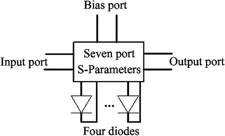
Fig.2 Doubler global optimization
2 Experimental results
The doubler circuit substrate is an ultra thin quartz substrate with thickness of 0.05mm, and the dielectric constant of 3.78. The circuit is mounted to the block with silver epoxy and the area is 3.3×0.5mm2. The split block is manufactured by brass and electroplate with gold. The doubler split block photo is given in Fig.3.

Fig.3 Photo of the doubler
The doubler measurement setup is presented in Fig.4. The input pump power of doublers is provided by BWO-W signal generator of ELVA-1, and it is precisely calibrated by millimeter and submillimeter power meter PM-4. As shown in Fig.5 and Fig.6, the highest measured conversion efficiency of 6.1% and the output power of 5.4mW are measured at 214GHz with the input power of 88mW, and the output power is higher than 4.1mW in 210~225GHz, and the typical measured efficiency is 4.5% in 200~225GHz. The maximum deviation between measured and simulated efficiency is about 3%, which may be caused by minor errors of diode physical dimension in simulation because the exact diode dimension is commonly unavailable, and the diode series resistance in simulation should be corrected empirically to achieve good agreement between calculated and experimental results. The unbalance of diode four anodes, block manufacture errors and the mounting alignment accuracy of the diode can also affect the performance of the doublers. It can be found from Fig.7 that the measured return loss is about -7dB and response is flat.

Fig.4 Measurement setup of the doubler
Table 1 illustrates some reported multipliers performance. Compared with Ref.[14], the proposed multiplier average value is superior, while bandwidth and efficiency are better than that of Ref.[15]. Compared to the multiplier in Ref.[16], which is optimized for fixed frequency; the proposed doubler has the advantage of wider bandwidth. Obviously, the designed doubler achieves the same level as reported papers.

Fig.5 Measured output power versus input power

Fig.6 Multiply efficiency
3 Conclusions
A 5.4mW and 6.1% efficiency fixed-tuned 214GHz frequency doubler is analyzed and designed with planar barrier Schottky diode, respectively. Full-wave analysis is carried out to find diode embedding impedances with lumped port to model the nonlinear junction. An iterative “divide and combine” design approach is adopted for circuit optimization. The optimized exported S-parameters of the circuit are used for multiplying efficiency analysis. To the doubler, the highest measured conversion efficiency of 6.1% and output power of 5.4mW are measured at 214GHz with input power of 88mW, and output power is higher than 4.1mW in 210~225GHz, the typical measured efficiency is 4.5% in 200~225GHz. The doubler is compact, fixed-turned, and high efficiency, which is very attractive for test instrument, frequency sources and corresponding application systems.
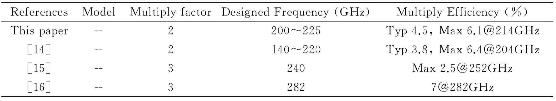
Table 1 Performance comparison
[1] Eisele H, Hadda G I. High-performance InP Gunn devices for fundamental-mode operation in D-band (110-170GHz).IEEETransactionsonMicrowaveWirelessComponentsLetters, 1995, 5(11): 385-387
[2] Eisele H, Hadda G I. Two-terminal millimeter-wave sources.IEEETransactionsonMicrowaveTheoryandTechniques, 1998, 46(6): 739-746
[3] Eisele H, Hadda G I. Potential and capabilities of two-terminal devices as millimeter and submillimeter-wave fundamental sources. In: IEEE MTT-S International Microwave Symposium Digest, Anaheim, USA, 1999. 933-936
[4] Bangert A, Schlechtweg M, Lang M, et al. W-band MMIC VCO with a large tuning range using a pseudomorphic HFET. In: IEEE MTT-S International Microwave Symposium Digest, San Francisco, USA, 1996. 525-528
[5] Uchida K, Matsuura H, Yakihara T, et al. A series of InGaP/InGaAs HBT oscillators up to D-Band.IEEETransactionsonMicrowaveTheoryandTechniques, 2001, 49(5): 858-865
[6] Winkler W, Borngr?ber J. LC-oscillator for 94 GHz automotive radar system fabricated in SiGe: BiCMOS technology. In: Gallium Arsenide Applications Symposium, Amsterdam, Netherlands, 2004. 45-46
[7] Campos R Y, Schw?rer C, Leuther A, et al. A D-band frequency doubler MMIC based on a 100-nm metamorphic HEMT technology.IEEETransactionsonMicrowaveWirelessComponentsLetters, 2005, 15(7): 466-468
[8] Campos R Y, Schw?rer C, Leuther A, et al. G-Band metamorphic HEMT-based frequency multipliers.IEEETransactionsonMicrowaveTheoryandTechniques, 2006, 4(7): 2983-2992
[9] Cao C H, Kenneth K O. A 140GHz fundamental mode voltage-controlled oscillator in 90nm CMOS tehnology.IEEETransactionsMicrowaveWirelessComponentsLetters, 2006, 16(10): 555-557
[10] Nicolson S T, Yau K H K, Chevalier P, et al. Design and scaling of W-band SiGe BiCMOS VCOs.IEEEJournalofSolid-StateCircuits, 2007, 42(9): 1821-1833
[11] Erickson N. High efficiency submillimeter frequency multipliers. In: IEEE MTT-S International Microwave Symposium Digest, Dallas, USA, 1990. 1301-1304
[12] Porterfield D W, Crowe T W, Bradley R F, et al. A high-power fixed-turned millimeter-wave balanced frequency doubler.IEEETransactionsMicrowaveTheoryTechnology, 1999, 47(4): 419-425
[13] Chattopadhyay G. Technology, Capabilities, and performance of low power Terahertz sources.IEEETransactionsonTerahertzScienceandTechnology, 2011, 1(1): 33-53
[14] Kiuru T, Dahlberg K, Mallat J, et al. Schottky frequency doubler for 140-220GHz using MMIC foundry process. In: Proceedings of the 7th European Microwave Integrated Circuits Conference, Amsterdam, Netherlands, 2012. 84-87
[15] Jones J R, Bishop W L, Jones S H, et al. Planar multibarrier 80/240-GHz heterostructure barrier varactor triplers.IEEETransactionsonMicrowaveTheoryandTechniques, 1997, 44(4): 512-518
[16] Vukusic J, Bryllert T, Olsen ?, et al. Monolithic HBV-based 282GHz tripler with 31mW output power.IEEEElectronDeviceLetters, 2012, 33(6): 800-802
Yao Changfei, born in 1982. He received his Ph.D degree from Southeast University in 2010. He now serves as a senior engineer in Science and Technology on Monolithic Integrated Circuits and Modules Laboratory, Nanjing Electronic Devices Institute. His work focuses on millimeter and submillimeter wave circuit and systems.
10.3772/j.issn.1006-6748.2015.01.012
*Supported by the 12th Five-year Defense Pre-research Fund of China (No. 51308030509).
*To whom correspondence should be addressed. E-mail: yaocf1982@163.comReceived on Sep. 2, 2013
 High Technology Letters2015年1期
- High Technology Letters的其它文章
- Research on assessing compression quality taking into account the space-borne remote sensing images*
- Filtered-beam-search-based approach for operating theatre scheduling*
- Exploiting PLSA model and conditional random field for refining image annotation*
- Maneuvering target tracking algorithm based on cubature Kalman filter with observation iterated update*
- Retrieval and analysis of sea surface air temperature and relative humidity*
- Data organization and management of mine typical object spectral libraries*