
Hybrid Aging Delay Model Considering the PBTI and TDDB
2015-02-13 01:57:23YongMiaoMaoXiangYiGuiMaoZhangandDaWenXu
Yong Miao, Mao-Xiang Yi, Gui-Mao Zhang, and Da-Wen Xu
Hybrid Aging Delay Model Considering the PBTI and TDDB
Yong Miao, Mao-Xiang Yi, Gui-Mao Zhang, and Da-Wen Xu
—With a 45 nm process technique, the shrinking silicon feature size brings in a high-k/metal gate which significantly exacerbates the positive bias temperature instability (PBTI) and time-dependent dielectric breakdown (TDDB) effects of a NMOS transistor. However, previous works presented delay models to characterize the PBTI or TDDB individually. This paper demonstrates that the delay caused by the joint effects of PBTI and TDDB widely differs from the cumulated result of the delay caused by the PBTI and TDDB, respectively, with the experiments on an inverter chain. This paper proposes a hybrid aging delay model comprising both the PBTI and TDDB effects by analyzing the relationship between the aging propagation delay and the inherent delay of the gate. Experimental results on the logic gates under 45 nm, 32 nm, 22 nm, and 16 nm CMOS technologies show that the maximum error between the proposed model and the actual value is less than 2.5%, meanwhile the average error is about 1.5%.
Index Terms—Circuit aging, positive bias temperature instability, time-dependent dielectric breakdown.
1. Introduction
Integrated circuits (ICs) have been developed more than 50 years under the prediction of the Moore’s law. With IC technologies improving and devices scaling, a series of reliability issues which accelerate the aging of the circuits have become increasingly critical. Especially for high-k (HK)/metal gates NMOS transistor, the positive bias temperature instability (PBTI) and time-dependent dielectric breakdown (TDDB) effects are the two biggest issues which affect the reliability of IC.
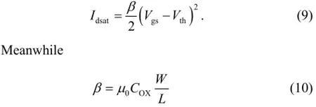
Firstly, regarding to the PBTI, the electron trapping in the bulk of the high-k oxidation layer is the main reason for the threshold voltage (Vth) shifts[1]. In recent years, researches on the PBTI are based on the high-k/metal gate transistor and can be roughly divided into two parts: One is the study on itself, the impact of PBTI on Vthhas been researched through trapping and de-trapping characteristics[2], meanwhile the methods for reducing ΔVthand creating delay models based on the ΔVthare discovered[3],[4]; the other researches focus on the joint effects considering PBTI and other aging effects, such as negative bias temperature instability (NBTI), TDDB, etc.[5]-[7].
Secondly, the TDDB effect degrades the oxide layer’s insulating properties aggressively, and finally makes complete conduction between the gate and the substrate[8]. As we know, the impact of TDDB on the device can be divided into two stages: Soft oxide breakdown and hard oxide breakdown. In the soft oxide breakdown phase, the device is still functional but the electrical properties, such as energy and delay, are changed. In the hard oxide breakdown phase, the leakage current increases exponentially and this increment will gradually lead to a permanent failure[9]. Currently, most of the researches on the TDDB have focused on studying the characteristics of static random access memory (SRAM) cells in the presence of soft oxide breakdown. The energy/delay drift in the SRAM due to the soft oxide breakdown was addressed in [10], and the impact of TDDB on the stability of SRAM was investigated in [11] and [12].
Since both the PBTI and TDDB occur primarily in NMOS transistors, some works comprising the PBTI and TDDB have been presented. The effect of adopting HfSiON on improving the PBTI and TDDB aware reliability was studied in [13], the intrinsic correlation between the PBTI and TDDB was addressed in [14]. However, combining both of them and discussing the impact on the delay have not been involved. This paper establishes a hybrid aging propagation model considering both the PBTI and TDDB in high-k/metal gate NMOS transistors for predicting the circuit aging delay.
The rest of this paper is organized as follows. Section 2 reviews related works including both the PBTI and TDDB models. Section 3 proposes our delay model considering both PBTI and TDDB. Section 4 is the experiments and analysis. Section 5 concludes the paper.
2. Model of PBTI and TDDB
2.1 PBTI
Currently, the aging effects of circuits can be mainly categorized into bias temperature instability (BTI), time-dependent dielectric breakdown (TDDB), hot carrier injection (HCI), and electromigration (EM) according to the different physical mechanisms. As well, the BTI effect can also be continuously divided into negative bias temperature instability (NBTI) and positive bias temperature instability (PBTI). The NBTI mainly occurs in the PMOS transistor while the PBTI occurs in the NMOS transistor. In ordinary silicon transistors, the effect of PBTI is much weaker than that of NBTI. So in the past 20 years, most of researchers have focused on the impact of NBTI. When the process geometry of integrated circuits scaled down to 45 nm and below, high-k materials begun to replace SiO2as gate oxide in order to solve the increasing serious leakage problems. And scientists have found out some specific metals, e.g. hafnium, to realize the high-k/metal gate. It is found that the Vthof the NMOS transistor changes more and more with the increase of time in the high-k/metal gate transistor, which indicates that the PBTI effect is becoming significant. Therefore, the PBTI starts to gain interest for recent years.
The PBTI effect can be described as follows. When the NMOS transistor gate is under the positive bias state, an interface trap will form on the oxide interface of the NMOS transistor, which results in a higher Vthand smaller drive current of the NMOS transistor. Therefore, the propagation delay of the gate goes to increasingly larger. The increasing delay easily causes timing violation. The referred model considering the PBTI proposed in [15] is adopted in this paper. Meanwhile, the degradation of threshold voltage ΔVthdue to the NBTI can be calculated as

where Vgis the gate voltage, n is found to be in the range of 0.1 to 0.2, and the value of m depends on stack details such as interfacial layer (IL) and high-k) thickness, with typical values in the range of 5 to 10. The constant A depends on the stress voltage and temperature.
2.2 TDDB
Time-dependent dielectric breakdown (TDDB), commonly termed gate oxide breakdown, is emerging as one of the most important sources of temporal degradation in CMOS devices[9]. For CMOS devices, thin gate oxides and saturating trend in supply voltage scaling result in a large electric field in the gate oxide, which eventually causes traps forming in the oxide interface and then the tunneling currents. As time increases, the tunneling currents further degrade the oxide and lead to the formation of more traps. Once enough traps are formed, they start affecting the electrical properties of the device.
The referenced TDDB model used in this paper was proposed in [16]. As shown in Fig. 1, if the TDDB appeared in M2n, it can be considered that there is an equivalent resistance RBDexisted between the gate and the source. The smaller the value of RBDis, the more significant TDDB effect there will be. And the equivalent resistance RBDalso affects the size of VBD.
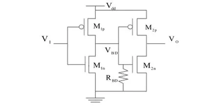
Fig. 1. Breakdown equivalent model.
When VBDis logic 1, V1is logic 0, the transistors of M1nand M2pare almost cut-off. From Ohm’s law, the current IBDis expressed as

where Vds,1pis the drain-to-source voltage of M1p. Then from C.T.sah equation, the current IBDalso can be expressed as
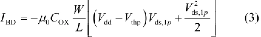
where μ0is the carrier mobility, COXis the gate oxide capacitance, W and L represent the channel width and length, respectively. Vthpis the threshold voltage for PMOS transistors. From (2) and (3), we can get Vds,1pas
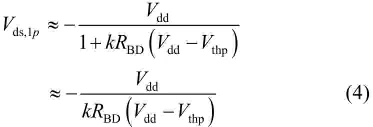
where k = μ0COXW/L and the degradation of VBDin this figure is |Vds,1p|, that is
where
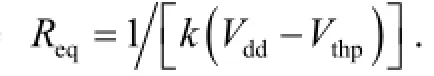
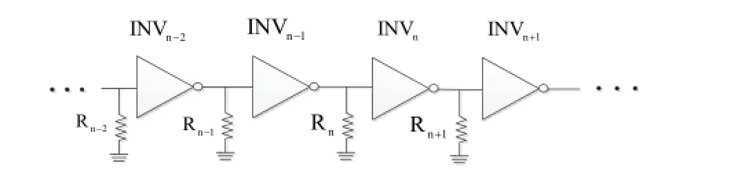
Fig. 2. Inverter chain schematic.
Reference [8] proposed a circuit-level TDDB delay model on the basis of [16], as shown in Fig. 2, in theinverter chain, the delay variation of INVnis expressed as

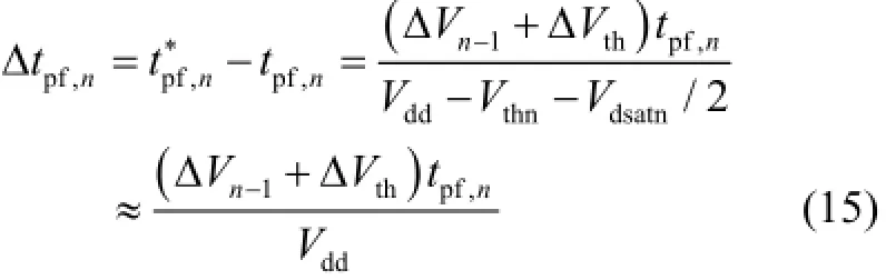
where tpf,nis the delay for the falling transition of INVnand tpr,nis for the rising transition. Vdsatnand Vdsatpare the saturation drain voltage of the NMOS and PMOS, respectively. ΔVn-1and ΔVnare the degradations of the input voltages caused by TDDB.
3. Delay Model for Both PBTI and TDDB
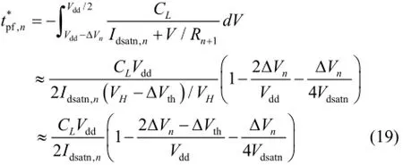
In Fig. 2, the delay of INVncan be divided into rising transition delay and falling transition delay. As described in [17], the rising transition delay is given as
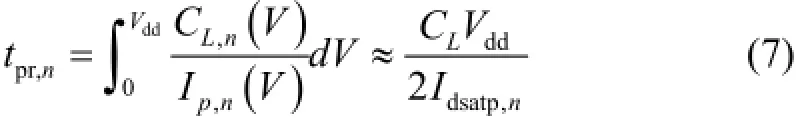
where CL,nis the effective capacitance of the INVnand can be considered as the constant CL, Ip,nis the charging current, we consider that it remains constant as Idsatp,n, which is the saturation current of PMOS transistors.
Similarly, the falling transition delay can be given as
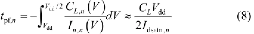
where In,nis the discharging current and we use Idsatn,nto instead of it, which is the saturation current of NMOS transistors. For INVn, ΔVthcaused by the PBTI, Rnand Rn+1caused by the TDDB can affect the time delay of INVn.
3.1 Influence of Rnand ΔVth
In a CMOS transistor, the saturation current is expressed as
where Vgsis the gate-source voltage, combined with v = μ0E and E = Vds/L, we can get that
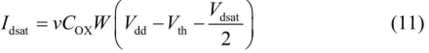
where v is the saturation velocity of carriers.
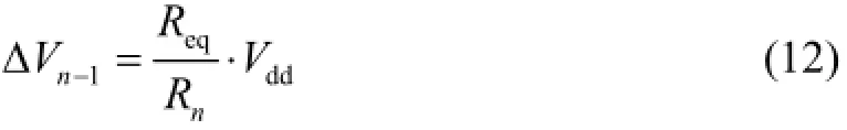
According to the analysis in section 2.2, when the TDDB appeared in INVn, that is the existence of Rn, the change value of the input voltage ΔVn-1of INVnis
With the existence of PBTI, we assume the degradation of the threshold voltage swing ΔVth, then we can get the saturation current of a NMOS transistor

as ΔVth<<Vddand ΔVn-1<<Vdd, we can derive the new propagation delay
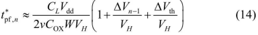
where VH= Vdd- Vthn- Vdsatn/2.
Therefore, the increase of the propagation delay for the falling transition can be expressed as
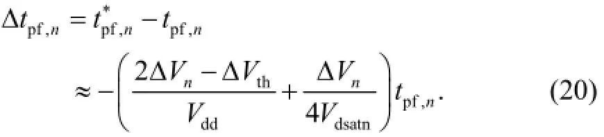
3.2 Influence of Rn+1and ΔVth
As Fig. 3 and Fig. 4 show, the existence of Rn+1can also affect the charging current and discharging current of INVn, that is, it can affect the delay of INVn.
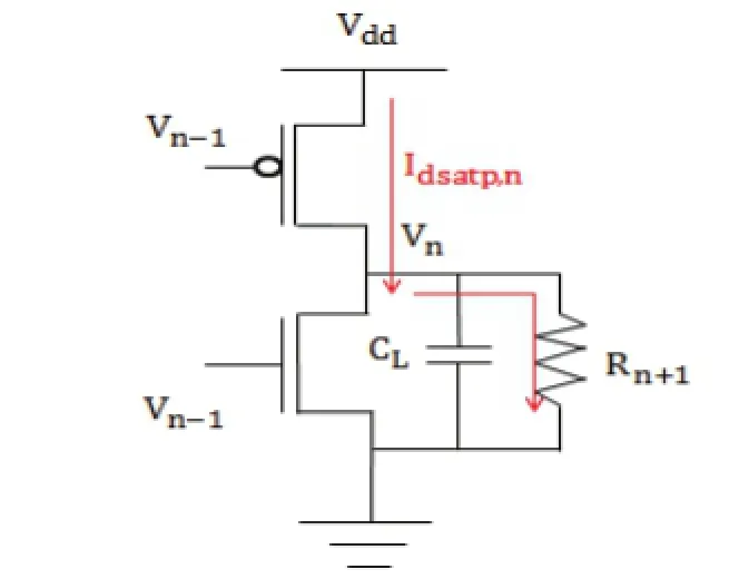
Fig. 3. Delay variation for rising with ΔVn.
Firstly, in Fig. 3, for the rising transition, Rn+1will bypass a portion of the current, the charging current can be given as Idsatp,n-V/Rn+1, and Idsatp,n>>V/Rn+1, where V is the voltage of Rn+1, and the delay for the rising transition can be described by
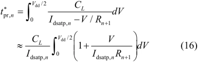
and the increase of the delay can be expressed as
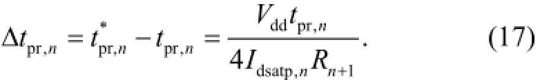
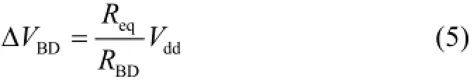
According to the analysis in Section 2.2, we know that ΔVn=VddReq/Rn+1, and Reqis approximately equal to Vdsatp/Idsatp,n, thus we can get
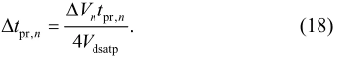
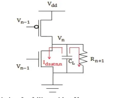
Fig. 4 Delay variation for falling with ΔVn.
Secondly, in Fig. 4, for the falling transition, the discharging current can be described as Idsatn,n+V/Rn+1for the existence of Rn+1. Meanwhile, with the increase of the threshold voltage for the PBTI, we assume the value is ΔVth, thus we can derive that
the delay variation is given that
From the above, considering both the PBTI and TDDB, the delay variation for the rising transition of INVnshould be

The delay variation for the falling transition of INVnshould be
So the delay for the INVnis
4. Results and Discussion
4.1 Comparison with Hspice Simulated Results
In this paper, we use the 4-stage inverter chain as benchmark. We assume that all of the equivalent resistances are the same, and the value is 50 k?, thus ΔVnare same for all the nodes. We also assume that all the inverters are the same, the delay of the inverter chain is

The model for propagation delay is validated against Hspice simulations for 45 nm, 32 nm, 22 nm, and 16 nm technology libraries[18]. The results are shown in Table 1, in which r% is the percentage of actual Δtpsimulated by the Hspice for the inherent delay, while m% is the percentage of Δtpcalculated by the proposed model for the inherent delay.
As shown in Table 1, the maximum error in the propagation delay of the inverter chain estimated using our analytical model is less than 2.5% as compared with the Hspice simulations. And through data analysis we know that simple TDDB mechanism may reduce the delay circuit for the value of (20). With the increase of ΔVthcaused by the PBTI, the reduction in the value of the circuit delay decrease shows that the PBTI effect will increase the circuit delay, but the degree is less than that of TDDB.
4.2 Comparison with Previous Model Calculated Results
In this section, we use the previous individual PBTI delay model[19]and TDDB delay model[8]to calculate their influence on the circuit respectively and compute their accumulated value directly, then compare with the proposed hybrid model. We still utilize the 4-stage inverter chain as our benchmark, and the equivalent resistances maintain 50 k?. The results are shown in Table 2, in which tPreis the delay calculated by the previous model,Δp is the difference between the previous model and the Hspice simulations, while Δh is the difference between the proposed hybrid model and the Hspice simulations.
As shown in Table 2, all the data show that the proposed hybrid model is more accurate than the previous model. It also can be seen from Table 2 that the bigger of ΔVthmeans the greater influence of PBTI and the more accurate of the hybrid model compared with the previous model.
The average errors and error variances of the previous model and hybrid model are calculated and shown in Fig. 5. As shown in Fig. 5 (a), the average errors of our hybrid model are smaller than the average errors of the previous model. It also can be seen that it is more accurate in 45 nm and 32 nm than that in 22 nm and 16 nm for the hybrid model. In Fig. 5 (b), for the previous model, all the error variances are bigger than the hybrid model excepted for that in 22 nm.
5. Conclusions
This paper proposes a hybrid aging-aware delay model considering both the PBTI and TDDB simultaneously. The experimental results show the proposed hybrid model andthe actual situation are highly consistent, and it is more accurately than the previous model. So it provides a relatively simple prediction algorithm for the circuit aging delay.

Table 1: Delay variation of 45 nm, 32 nm, 22 nm, and 16 nm
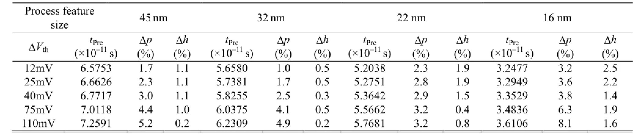
Table 2: Error of delay variation
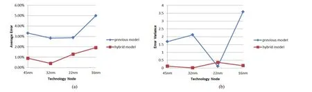
Fig. 5. Error analysis: (a) average errors and (b) error variances.
[1] K. Zhao, J. H. Stathis, A. Kerber, and E. Cartier, “PBTI relaxation dynamics after AC vs. DC stress in high-k/metal gate stacks,” in Proc. of 2010 Intl. Reliability Physics Symposium Conf., 2010, pp. 50-54.
[2] W. L. Lin, Y. J. Lee, W. C. Lo, Y. T. Hou, K. C. Lin, and T. S. Chao, “Trapping and de-trapping characteristics in PBTI and dynamic PBTI between HfO2 and HfSiON gate dielectrics,”in Proc. of 2008 Intl. Symposium on the Physical and Failure Analysis of Integrated Circuits Conf., 2008, pp. 1-4.
[3] C. Schlunder, H. Reisinger, S. Aresu, and W. Gustin, “On the PBTI degradation of pMOSFETs and its impact on IC lifetime,” in Proc. of 2011 Integrated Reliability Workshop Final Report Conf., 2011, pp. 7-11.
[4] K. Zhao, J. H. Stathis, B. P. Linder, A. Kerber, and E. Cartier,“PBTI under dynamic stress: From a single defect point ofview,” in Proc. of 2011 Intl. Reliability Physics Symposium Conf., 2011, pp. 4A.3.1-4A.3.9.
[5] S. Kiamehr and F. Firouzi, “Aging-aware timing analysis considering combined effects of NBTI and PBTI,” in Proc. of 2013 Intl. Symposium on Quality Electronic Design Conf., 2013, pp.53-59.
[6] J. -J. Kim, B. P. Linder, R. M. Rao, K. A. Jenkins, and C. H. Kim, “Reliability monitoring ring oscillator structures for isolated/combined NBTI and PBTI measurement in high-k metal gate technologies,” in Proc. of 2011 Intl. Reliability Physics Symposium Conf., 2011, pp. 2B.4.1-2B.4.4.
[7] M. Sato, S. Kamiyama, Y. Sugita, and T. Matsuki,“Negatively charged deep level defects generated by Yttrium and Lanthanum incorporation into HfO2 for Vth adjustment, and the impact on TDDB, PBTI and 1/f noise,”in Proc. of 2009 Intl. Electron Devices Meeting Conf., 2009, pp. 1-4.
[8] H. Luo, X. M. Chen, J. Velamala, Y. Wang, Y. Cao, and H. Z. Yang, “Circuit-level delay modeling considering both TDDB and NBTI,” in Proc. of 2011 Intl. Symposium on Quality Electronic Design Conf., 2011, pp.1-8.
[9] M. Alam, B. Weir, and P. Silverman, “A study of soft and hard breakdown—Part I: Analysis of statistical percolation conductance,” IEEE Trans. on Electron Devices, vol. 49, no. 2, pp. 232-238, 2002.
[10] H. Wand, M. Miranda, F. Catthoor, and W. Dehaene,“Impact of random soft oxide breakdown on SRAM energy/delay drift,” IEEE Trans. on Device and Materials Reliability, vol. 7, no. 4, pp. 581-591, 2007.
[11] B. Kaczer, R. Degraeve, P. Roussel, and G. Groeseneken,“Gate oxide breakdown in FET devices and circuits: From nanoscale physics tosystem-level reliability,” in Proc. of 2007 Workshop on Dielectrics in Microelectronics Conf., 2007, pp. 559-566.
[12] R. Rodriguez, J. Stathis, B. Linder, S. Kowalczyk, and C. Chuang, “The impact of gate-oxide breakdown on SRAM stability,” IEEE Electron Device Letters, vol. 23, no. 9, pp. 559-561, 2002.
[13] M. Sato, N. Umezawa, J. Shimokawa, H. Arimura, S. Sugino, and A.Tachibana, “Physical model of the PBTI and TDDB of La incorporated HfSiON gate dielectrics with pre-existing and stress-induced defects,” in Proc. of 2008 Intl. Electron Devices Meeting Conf., 2008, pp. 1-4.
[14] J. Q. Yang, M. Muhammad, K. Joshi, S. Mukhopadhyay, and J. F. Kang, “Intrinsic correlation between PBTI and TDDB degradations in nMOS HK/MG dielectrics,” in Proc. of 2012 Intl. Reliability Physics Symposium Conf., 2012, pp. 5D.4.1-5D.4.7.
[15] D. P. Ioannou, E. Cartier, Y. Wang, and S. Mittl, “PBTI response to interfacial layer thickness variation in Hf-based HKMG nFETs,” in Proc. of 2010 Intl. Reliability Physics Symposium Conf., 2010, pp. 1044-1048.
[16] M. Choudhury, V. Chandra, R. Aitken, and K. Mohanram,“Analytical model for TDDB—based performance degradation in combinational logic,” in Proc. of 2010 Design, Automation & Test in Europe Conf. & Exhibition Conf., 2010, pp. 423-428.
[17] M. Hashimoto, J. Yamaguchi, T. Sato, and H. Onodera,“Timing analysis considering temporal supply voltage fluctuation,” in Proc. of 2005 Asia and South Pacific Design Automation Conf., 2005, pp. 1098-1101.
[18] Z. Adil, G. Kapil, V. Ankit, and R. Ashish, “Design & simulation of CMOS inverter at nanoscale beyond 22 nm,”in Proc. of 2013 Intl. Journal of Emerging Science and Engineering Conf., 2013, pp.83-87.
[19] Y. Wang, X. M. Chen, W. P. Wang, Y. Cao, Y. Xie, and H. Z. Yang, “Leakage power and circuit aging cooptimization by gate replacement techniques,” IEEE Trans. on Very Large Scale Integration (VLSI) Systems, vol. 19, no. 4, pp. 615-628, 2011.

Yong Miaowas born in Anhui Province, Chinain 1990. He received the B.S. degree in electronic science and technology from Hefei University of Technology, Hefei in 2012. He currently is a postgraduate of Hefei University of Technology. His research is to develop the circuit innate aging-tolerant ability by innovative aging-tolerant design methods for nanometer scale integrated circuits.

Mao-Xiang Yiwas born in Anhui Province, China in 1964. He received the Ph.D. degree from Hefei University of Technology. He currently is a professor with the School of Electronic Science & Applied Physics, Hefei University of Technology. His main research interests include the design and test on the very large scale integrated circuites (VLSI) and application of microelectronics and computer.

Gui-Mao Zhangwas born in Guangxi Province, China, in 1988. He received the B.S. degree in electronic information science and technology from Hunan University of Science and Technology, Changsha in 2012. He currently is a postgraduate with Hefei University of Technology. His research interests include circuit aging prediction and protection methods for aging.

Da-Wen Xuwas born in 1986. He received the B.S. degree in computer science from Xi’dian University, Xi’an in 2007, and the M.S. and Ph.D. degrees from the Institute of Computing Technology, Chinese Academy of Science, Beijing in 2009 and 2013, respectively. He is currently an associate professor with Hefei University of Technology. His current research
interests include heterogeneous computing, VLSI design and test, and reliable system.
Manuscript received November 19, 2014; revised January 25, 2015. This work was supported by the National Natural Science Foundation of China under Grant No. 61371025 and No. 61274036.
Y. Miao is with the School of Electronic Science and Applied Physics, Hefei University of Technology, Hefei 230009, China (Corresponding author e-mail: myfly627@163.com).
M.-X. Yi, G.-M. Zhang, and D.-W. Xu are with the School of Electronic Science and Applied Physics, Hefei University of Technology, Hefei 230009, China (e-mail: mxyi126@126.com; zhangguimao2008 @163.com; xudawen@gmail.com).
Digital Object Identifier: 10.11989/JEST.1674-862X.411191
 Journal of Electronic Science and Technology2015年3期
- Journal of Electronic Science and Technology的其它文章
- Energy Management Strategies for Modern Electric Vehicles Using MATLAB/Simulink
- Time-Efficient Identification Method for Aging Critical Gates Considering Topological Connection
- Residual Phase Noise and Time Jitters of Single-Chip Digital Frequency Dividers
- A Methodology to Measure the Environmental Impact of ICT Operating Systems across Different Device Platforms
- Enhancement of Distributed Generation by Using Custom Power Device
- Influence of Taxation on Supply and Demand in Tomorrow’s Crowd Energy Paradigm