
Design of LED display based on FPGA
2013-11-01 01:26:24ZHOUYuanyuan周苑苑LVChangzhi呂常智GAOTingXINGuozhi辛國(guó)治
關(guān)鍵詞:山東
ZHOU Yuan-yuan (周苑苑), LV Chang-zhi (呂常智), GAO Ting (高 廷), XIN Guo-zhi (辛國(guó)治)
(College of Information and Electrical Engineering, Shandong University of Science and Technology, Qingdao 266590, China)
Design of LED display based on FPGA
ZHOU Yuan-yuan (周苑苑), LV Chang-zhi (呂常智), GAO Ting (高 廷), XIN Guo-zhi (辛國(guó)治)
(College of Information and Electrical Engineering, Shandong University of Science and Technology, Qingdao 266590, China)
If single chip micro computer controls light-emitting diode (LED), it needs abundant peripheral resources, but in this way, it is not convenient to be expanded, modified and maintained. In order to overcome these shortcomings, field programmable gate array (FPGA) is used to control LED. The hardware design uses low power consumption and high performance device EP1C6Q240C8. Quartus II is the software development environment. There are three modules built under the software development environment: divided clock module, word stock module and LED dot matrix display module, and these independent modules are connected to be a whole system. Finally, 32×64 dot matrix display is realized successfully. It is convenient for the customer to adjust the three independent modules according to actual demands and it is easier to realize online updation.
field programmable gate array (FPGA); EP1C6Q240C8; light-emitting diode (LED); dynamic display
With the development of economy and science, light-emitting diode (LED) has been used widely.
There are two prominent characteristics of LED dot matrix display control, one is a large quantity of data, the other is high processing speed[1]. However, the existing function of processing system is so simple that if it achieves different functions, it has to modify content through cockamamie process, which is against enhancing efficiency of development.
Now, FPGA system design has began to enter the new era of “chip programmable system”, its characteristics include high density and low power consumption[2]. International companies are expanding its IP so that it can provide optimized resources and expand the market. LED dot matrix controller based on FPGA has broad application prospects[3]. It can be easily upgraded through changing FPGA internal hardware logic which can be downloaded online from the network.
Based on the above advantages, Cyclone II EP1C6 of Altera FPGA is chosen as controller to control LED dot matrix display. The main research is:
1) Hardware circuit design, including LED circuit, FPGA control circuit, power supply, etc.
2) Simulation of each module, including clock circuit, word stock and LED display, etc.
3) Based on Quartus Ⅱ development platform, by using VHDL and top design method, FPGA control circuit is realized.
The whole design diagram based on FPGA controller is shown in Fig.1i.
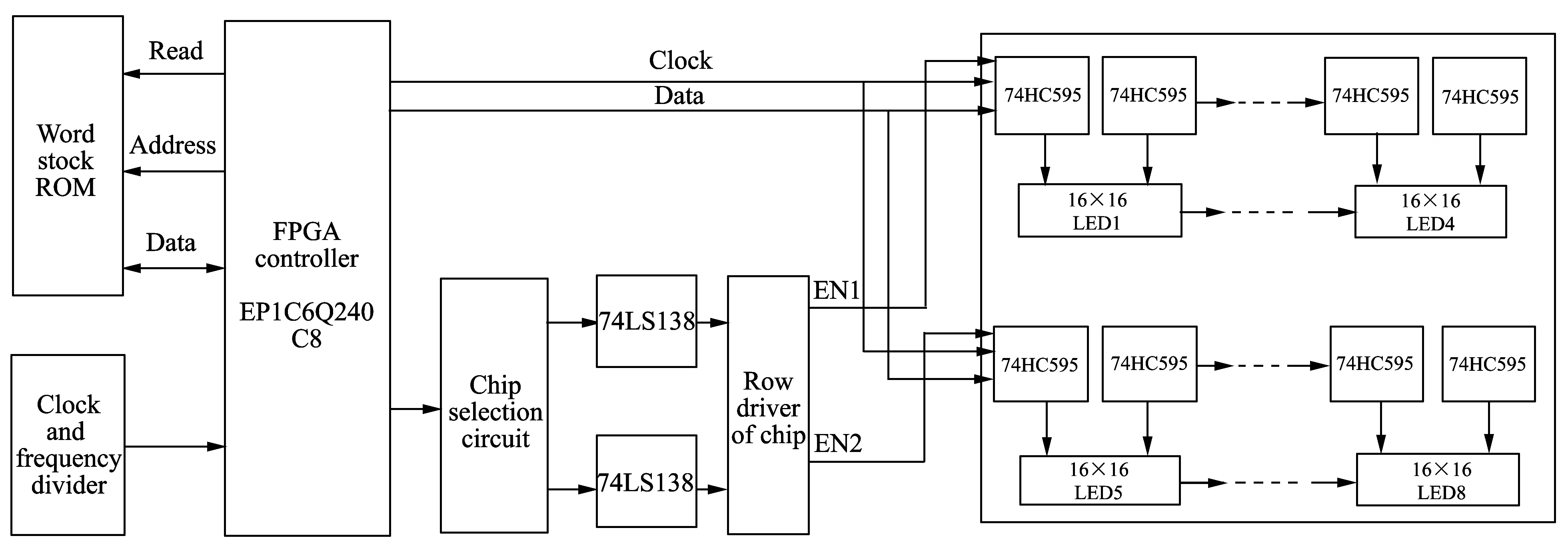
Fig.1 Design diagram based on FPGA
1 Design of hardware circuit
1.1 LED dot matrix module
In this paper, the LED dot matrix is common anode. 64×32 LED dot matrix module is got by connecting four 16×16 LED dot matrix.
The public interface serves as LED row control, and the row scanning signal can control multiple LED. Before arriving of the row scanning signal, it has to go through a driver chip — 4953[4]. Through the decoding circuit, the row scanning decides which row to display. The decoder chip is 74LS138[5]. The column scanning circuit uses the shift-register — 74HC595[6]with latch. Row control circuit of LED is shown in Fig.2.
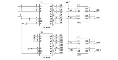
Fig.2 Row control circuit of LED
Column control circuit of LED is illustrated in Fig.3. Its main function is to send the word need to be displayed to LED cathode. Combining with row control circuit, LED display is realized.
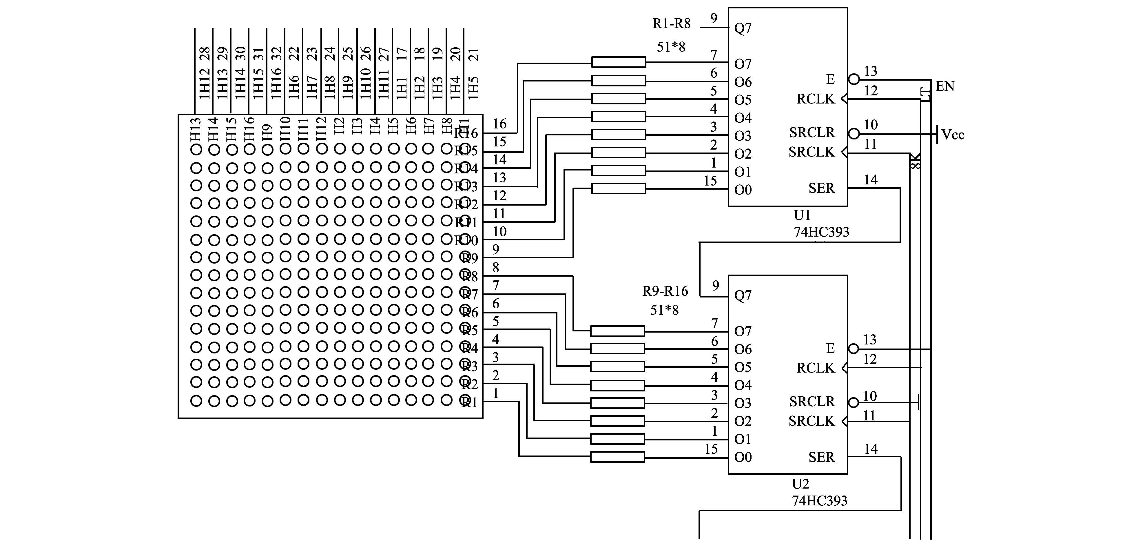
Fig.3 Columm control circuit of LED
1.2 FPGA configuration circuit
The chip of Cyclone has three configuration methods[7]: active serial configuration (AS) mode, passive serial configuration (PS) mode and joint test action group (JTAG). Above three methods are decided by two-bit model code, as shown in Table 1.
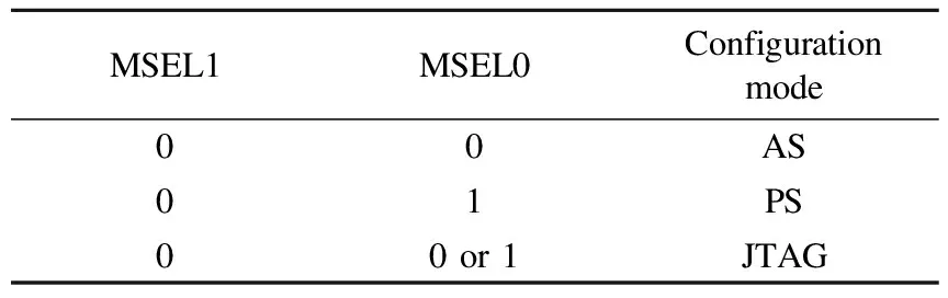
Table 1 Configuration mode of Cyclone
In this paper, AS plus JTAG is the best choice. JTAG module is used to debug so that the program has been debugged correctly.AS module downloads the program to the chip. The chip of Cyclone supports USB cable download. One side of the cable connects the USB of PC, the other side connects circuit socket. Download speed is faster than Byte Blaster II.
1.3 Design of power circuit
The external power is 7.4 V. The power of FPGA I/O is 3.3 V. The power of core is 1.5 V.
In order to convert 7.4 V into 1.5 V, the circuit is designed as shown in Fig.4.
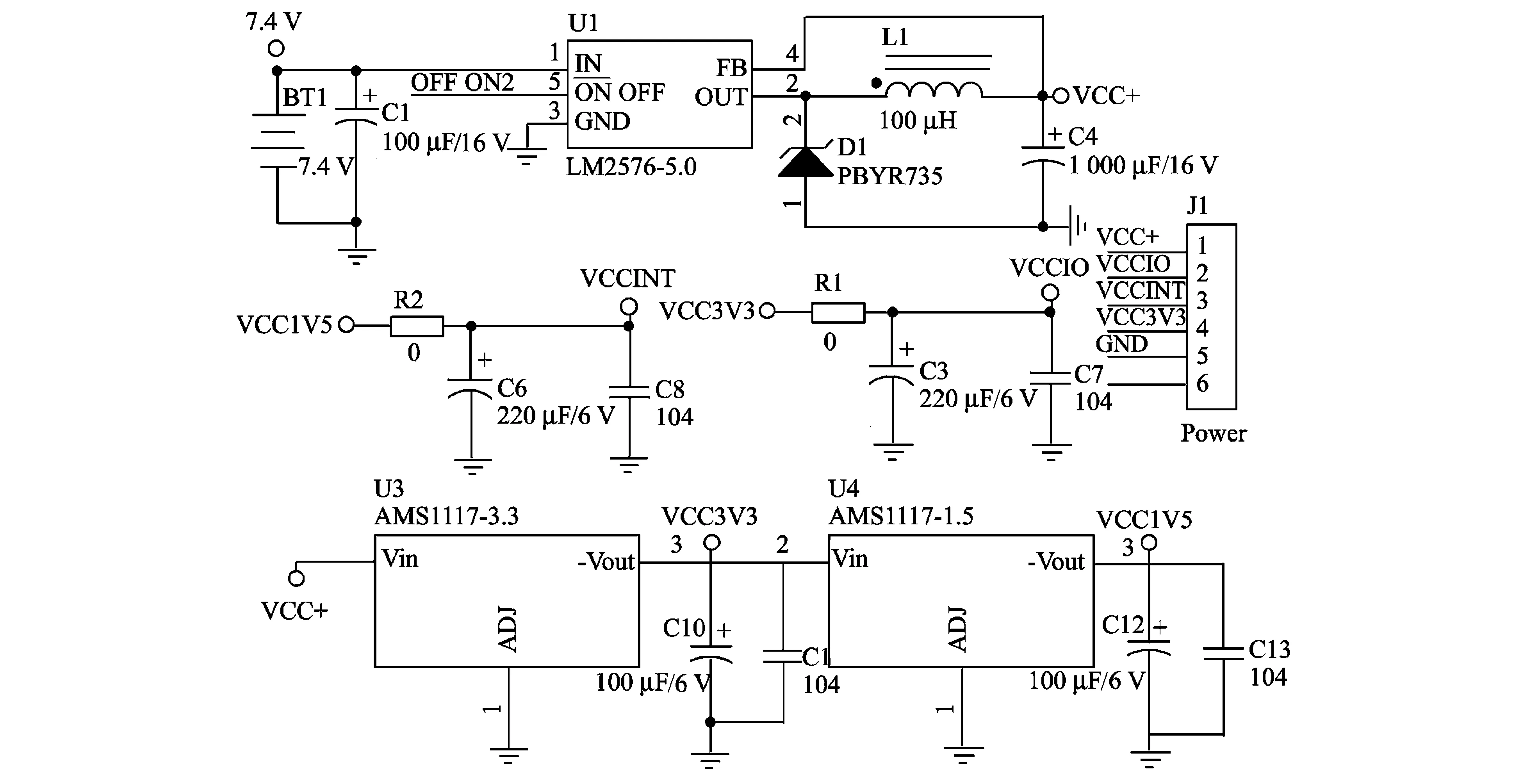
Fig.4 Power circuit
2 Software design
The design of software are consisted of five parts, this is obtaining three kinds of clock, words stock, the design of divided frequency, LED dot matrix display and system top layer design.
2.1 Three kinds of clock
The time sequence of row control is obtained on the basis of time sequence of 74HC595. The flowchart is shown in Fig.5.
It is time to explain the function of the three clocks.
S_in: data shift clock.
H_clk: in order to change address of data rom and renew LED data, a rising edge is set after every eight S_in clock.
LT_in: data latch clock, after sixty-four S_in clock, set a latch and at the same time the row address adds one.
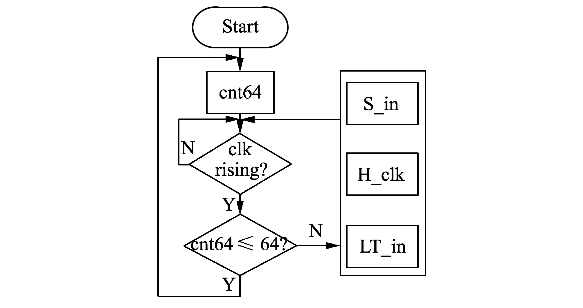
Fig.5 Flowchart of clock
According to the above principles, in Quartus II, use VHDL to program and package a module, shading the structure of inside circuit. The clock module named My_clk is shown in section 2.5.
2.2 Word stock
Dot matrix display is based on glyph code. In FPGA, LPM_ROM macro block is used for generating glyph code.
Design ideas for words stock are as follows:
1) Store 256 8-bit data in ROM.
2) Design 8-bit address pointer.
3) After eight clocks, the address pointer adds one, and read a glyph code.
The format of data of LPM_ROM contains .mif and .hex. In this paper .hex is chosen. Contents of words stock are “山東科大lys_skd”. The word stock module named R_data is shown in section 2.5.
2.3 Design of different clock frequency[10]
When LED is in dynamic scanning, if the frequency is too high, output data may have mistakes. Conversely, if the frequency is too low, LED display is unstable. So if the frequency is controlled well, stable display characters can be realized.
In this paper, phase-locked loops (PLL) of Quartus II can achieve frequency multiplication and frequency division by setting parameters directly[9].
The divided frequency module named freq_div is shown in section 2.5.
2.4 LED dot matrix display
The data of hardware circuit is output in a serial way. So data in ROM must be read bit by bit and clock signal is connected with line control signal. Characteristics of hardware circuit include:
1) The function of the shift-register.
2) Set a latch after the data has been output.
3) Control two pieces of LED dot matrix display
through changing the status of EN1 and EN2.
4) In order to display stably, once the scanning is over, then return automatic and scan again.
The flowchart is shown in Fig.6.
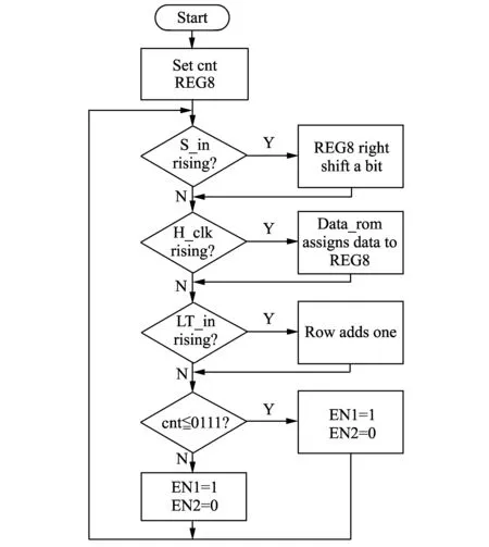
Fig.6 Flow chart of LED dot matrix display
The LED dot matrix display module named display is shown in section 2.5.
Fig.7 presents the result of LED dot matrix display simulation.
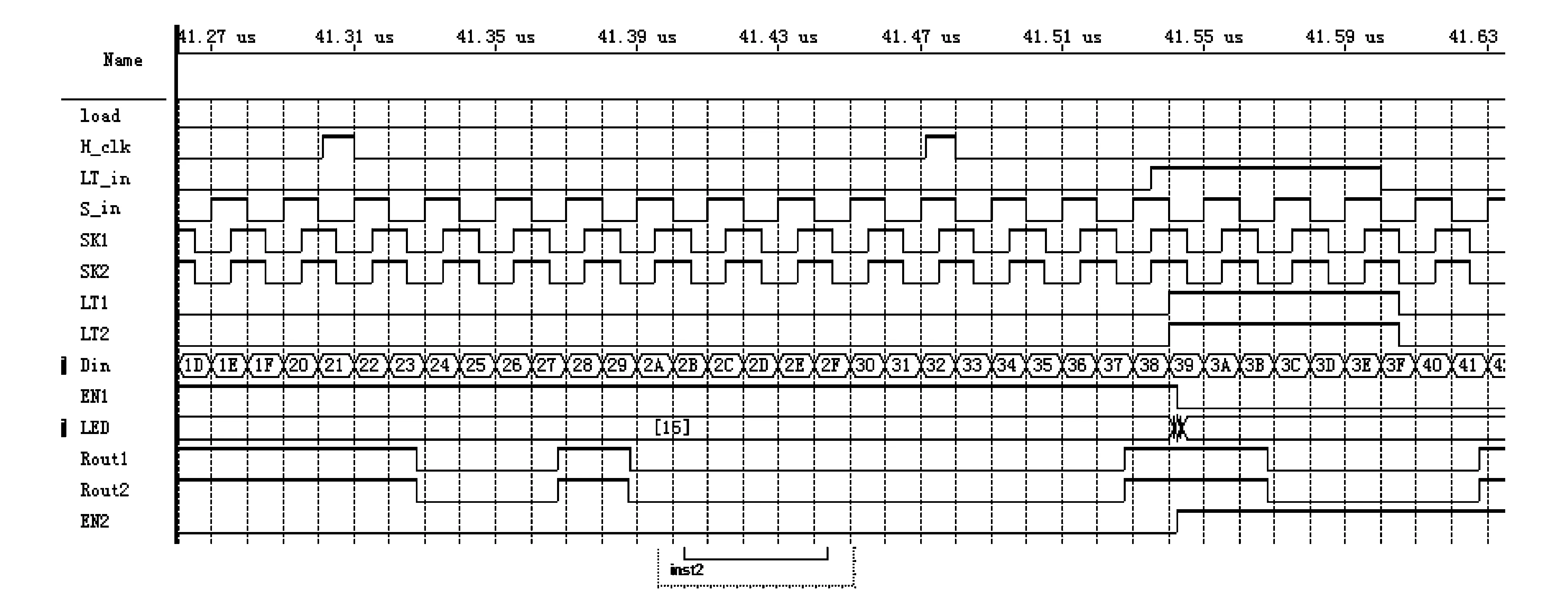
Fig.7 Simulation results of LED dot matrix display
Load is the reset signal, and it functions in low level. Rout1 and Rout2 are the outputs of above LED and below LED, respectively, EN1 and EN2 function in high level on-off control of LED. If EN1 is in high level, the above LED functions. S_in is assigned to SK1 and LT_in is assigned to LT1, which function in high level. Similarly, If EN2 is in high level, the below LED functions. S_in is assigned to SK2 and LT_in is assigned to LT2, which function in high level. Din is the content that is to be displayed in LED. When H_clk is in high level, Din is read, otherwise Din is unreadable. LED decides which row is going to be displayed.
2.5 Top layer design of the system
Connecting the four modules above as a whole, the system design principle diagram is shown in Fig.8.
The top layer design module is shown in Fig.9.
Fig.9 shows the whole software diagram, which is connected with independent modules that are generated by the previous software design. It is convenient to revise these modules, and thereby improve the efficiency.
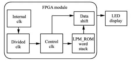
Fig.8 Module diagram of LED dot matrix display

Fig.9 Top layer design module
Fig.10 is the simulation results of Fig.8. The chart shows that the timing sequence is right. Row address is controlled correctly. The simulation results is consistent with the expected.
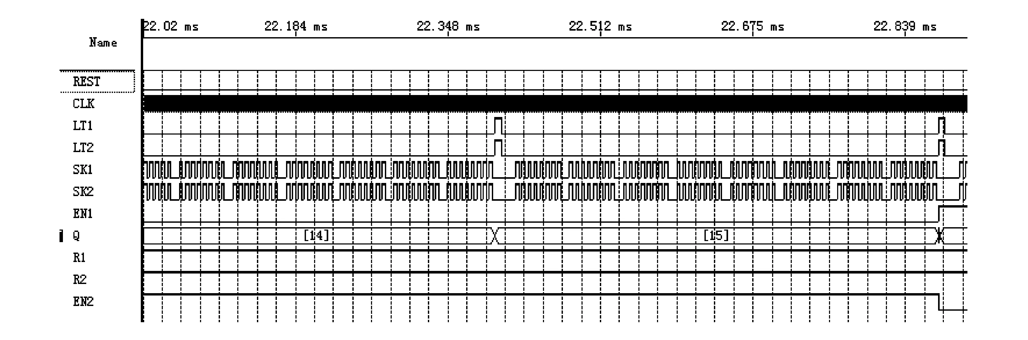
Fig.10 Simulation results of top layer design module
3 Test results
Downloading the program to EP1C6Q240C8 of FPGA, the test result is shown in Fig.11, it is the same as the expected.
4 Conclusion
As we know, single chip microcomputer has many advantages to control LED display[10], for example easy programming, low cost. But there are also disadvantages. When LED dot matrix is bigger, clock frequency required will be too higher to complete dynamic scan. I/O ports are used too many to achieve other functions at the same time. LED display is not stable. Realize online upgrade unfavorably.

Fig.11 Test results
Compared with signal chip microcomputer, FPGA could solve its shortages and optimize other functions making LED display more convenient, higher efficient. But there are several points to be paid attention to:
1) In order to display stably, the time sequence must be precise, or display will be chaos.
2) The power driver matching is also important.
Before the design, power circuit must be devise well in advance.
Design process and concrete procedures of LED display based on FPGA are introduced in the paper. In addition, the results of software simulation are presented clearly. In practical applications, this design can work effectively and steadily and meet the project's needs.
[1] ZHANG Yu-jie, MA Li-yun, ZHANG He-yan. The design of LED display control system based on ARM and FPGA. Computer Measurement & Control, 2009, (12): 24-32.
[2] LIU Jing. LED lighting system research and design. Yan’an: Yan’an University, 2009.
[3] ZHAO Xin-qing, LOU Jian-an. The application of LED based on FPGA. Development and Application of DSP, 2007, (23): 6-9.
[4] Fairchild Semiconductor Corporation. FDS4953 data sheet, 1999, 2(1): 17-20.
[5] Fairchild Semiconductor Corporation.74LS138 data sheet, 2000, 20(3): 12-23.
[6] Philips Corporation. 74HC595 data sheet, 2003, 6(4): 1.
[7] LV Chang-zhi, FAN Di. The controller of LED dot matrix display. Microcomputer Information, 2006, (1): 45-50.
[8] ZHANG Yi, YUE De-cai. LED intelligent display scanning circuit. Electronic and Automation, 1996, (2): 32-35.
[9] MEI Jian-chao. Sequence convergence and clock switching in FPGA designing. Science, 2011, (1): I0127-I0129.
[10] SONG Fen. The research and control technology of LED display based on AVR. Nanjing: Nanjing University of Science and Technology, 2009.
date: 2012-09-04
ZHOUYuan-yuan (oio-oio@yeah.net)
CLD number: TN873 Document code: A
1674-8042(2013)01-0077-06
10.3969/j.issn.1674-8042.2013.01.017
猜你喜歡
新航空(2023年9期)2023-09-18 18:59:16
金橋(2022年6期)2022-06-20 01:35:36
金橋(2022年4期)2022-05-05 06:10:00
走向世界(2022年3期)2022-04-19 12:38:54
金橋(2022年3期)2022-03-29 01:16:24
金橋(2022年3期)2022-03-29 01:16:20
中學(xué)生數(shù)理化·八年級(jí)物理人教版(2021年5期)2021-11-22 07:57:50
金橋(2021年6期)2021-07-23 01:27:06
能源(2020年10期)2020-11-13 07:05:40
學(xué)生天地(2020年31期)2020-06-01 02:32:24
 Journal of Measurement Science and Instrumentation2013年1期
- Journal of Measurement Science and Instrumentation的其它文章
- Acetonitrile (CH3CN) and methyl isocyanide(CH3NC) adsorption on Pt(111) surface: a DFT study
- Randomized Kaczmarz algorithm for CT reconstruction
- An improved ant colony algorithm and its application in optimal routing problem
- Digital FIR filter design for bio-signal processing system
- Odorant discrimination using functional near-infrared spectroscopy of the main olfactory bulb in rats
- Techniques trend analysis of propagating laser beam quality measurement