
Design of MEMS C-Band Microstrip Antenna Array Based on High-Resistance Silicon for Intelligent Ammunition
2013-07-29 09:43:10XueZhaoandXiaoMingLiu
Xue Zhao and Xiao-Ming Liu
1.Introduction
Microstrip antennas have been widely used in satellite communications,mobile phones,unmanned aerial vehicle(UAV)and weapons because of the attractive features of low profile,light weight,easy fabrication process,and conformability[1].In the intelligent transformation of ammunition,the controlling system can control the impact point of the ammunition by controlling the opening time of damping plate on the ammunition[2].So there must be units for sending and receiving signals and the most important component is antenna[3].Compared with the traditional machinery,the micro-sensors,micro-execution,signal processing and control circuitry,communications interface,and power supply components of micro-electro-mechanical systems(MEMS)can be integrated on a silicon chip by using MEMS technology,so the size of the system is smaller and it has better electrical properties,strength,and hardness[4]–[6].Thus,the automation,intelligent degree and level of reliability of the system can be improved by MEMS technology.Due to the very limited space on the bomb,it is very suitable for using MEMS and micro fabrication technology to design and manufacture microstrip antennas.An antenna that is manufactured by MEMS technology and precision machining technology has a lot of advantages in dimension,capability,price,and so on[7].However,the gain and efficiency of the conventional patch antenna are low and poor[8].In this paper,the performance of the antenna is improved by the following two ways:the first is to change the material of substrate,by using high-resistance silicon instead of conventional silicon;the second is to optimize the structure of the antenna.A cavity has been designed in the substrate to improve the gain and reduce the weight of the antenna.
2.Design Structure of Microstrip Antenna Array
A microstrip antenna array is made up of the substrate,patch,feed line,power splitter,ground plane,and so on.
2.1 Substrate
According to the research and analysis,it is found that the energy input to the antenna is absorbed but not radiated out when low-resistance silicon is used as the material of the substrate.In order to get better radiation characteristics,high-resistance silicon is used as the material of the substrate.The bulk conductivity is 0.0345 S/m.The resistance of silicon is 2900 Ω·cm.The thickness of the substrate has a significant impact on the bandwidth and the efficiency of the antenna.Increasing the thickness of the substrate can improve the bandwidth and the efficiency but the size and the weight of the antenna are also increased.Finally,the thickness of the substrate is designed as 0.450 mm because of the limiting factor of the specifications of the actual silicon thickness and MEMS processes.
An air cavity is designed under the patch in the substrate to reduce the equivalent permittivity of silicon,and there are advantages for a)increasing the total gain of the antenna,b)reducing the weight of the antenna,and c)helping to reduce the temperature of the antenna when it works in high-power condition.The structure of the microstrip antenna array is shown in Fig.1.
The equivalent permittivity εrcan be computed by
From(1),we know that the larger the thickness of the air cavity is,the smaller the equivalent permittivity is,and the higher the efficiency of the antenna is.But the thickness of the cavity cannot be designed very large because silicon is brittle material.When the thickness of the air cavity is 0.225 mm,the antenna has better electrical properties and much easier for manufacturing.The value of the equivalent permittivity computed from(1)is 1.845.
2.2 Patch
The material of patch is gold.When the relative dielectric constant εris decreased,the size of the patch will be increased.The size of the patch is determined by the center frequency of the antenna,and it is directly related to the gain pattern of the radiating element and the radiation efficiency.The width of the patch can be computed from(2)[9].
where W is the width of the patch,c is the speed of light,and fris the center frequency of the antenna.
The length of patch is computed by
where h(the thickness of the high-resistance substrate)equals to 0.450 mm and frequals to 4.5 GHz.Computing from(2)and(3),the width of the patch is 27.948 mm and the length of the patch is 19.663 mm.In this paper,the C-band microstrip antenna array is designed as circular polarization so that the width of the patch must be equal to the length.At last,the length of the patch is 27.948 mm.But all the calculated data are not to be very accurate.They will be adjusted in the simulation.
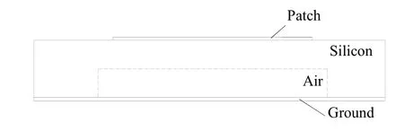
Fig.1.Structure of the microstrip antenna array.
2.3 Feed Line
A method of edge-fed microstrip line is designed in the antenna for providing energy.The impedance of antenna feed line is 50 Ω.The structure of microstrip antenna feeder is shown in Fig.2.
The width of antenna feed line can be computed by[10]
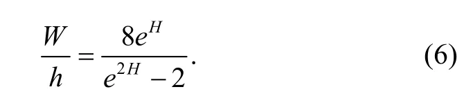
where e is the natural logarithm and H is the filling factor,its range is from 0 to 1.
2.4 Power Splitter
The gain of antenna can be improved by building an antenna array when the gain of single microstrip antenna element is relatively low.The power splitter is used in the shunt feed antenna array as dividing input signal energy into two or more outputs[11].The structure of conventional T-shaped power splitter is shown in Fig.3.It is difficult to manufacture microstrip lines when the size is small.An improved T-shaped power splitter is designed in this paper and the structure is shown in Fig.4.It is easier to manufacture and match the impedance.Finally,the network of feed is designed as Fig.4.The size of the microstrip antenna array is shown in Fig.5.

Fig.2.Microstrip-line diagram.
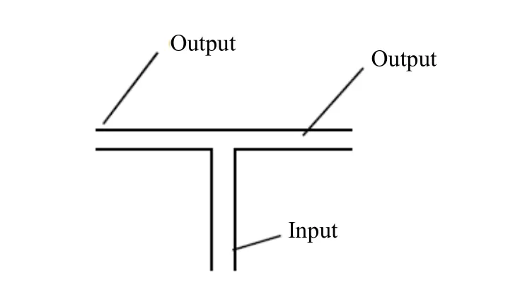
Fig.3.T-shaped power splitter.

Fig.4.Network of feed.
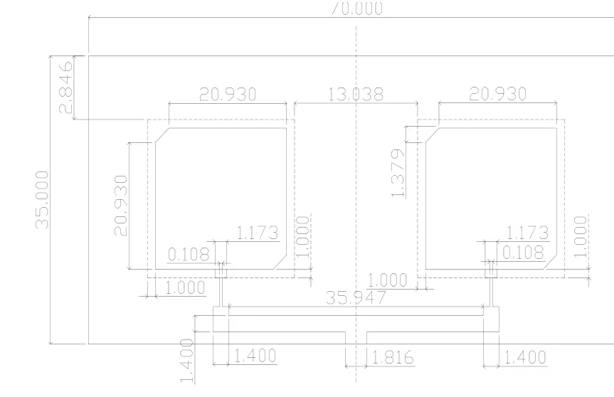
Fig.5.Size of the microstrip antenna array.
3.Analysis of Microstrip Antenna Array
A microstrip antenna array is designed to meet the demands of gain and power for long distance communication.The simulation model of the microstrip antenna array in high frequency structure simulator(HFSS)is shown in Fig.6.
The microstrip array antenna is simulated by HFSS.The width and the length of the patch are modified as 22.309 mm after optimizing.On the one hand,when low-resistance silicon(the resistance is 50 Ω·cm)is used as the material of the substrate,little energy is radiated out and there is a great loss in substrate.The chart of S11shown in Fig.7 indicates that is no resonant frequency.On the other hand,when there is not an air cavity in the substrate,the size of antenna can be reduced to 10.05 mm,but the gain of antenna is also very low.The highest gain is only –23.88 dB as shown in Fig.8.

Fig.6.Structure of array antenna.
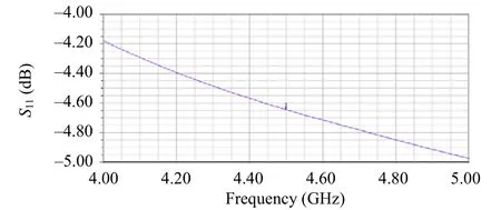
Fig.7.S11of low-resistant silicon substrate.

Fig.8.Gain of antenna array without air cavity.

Fig.9.S11of high-resistance silicon substrate with air cavity.
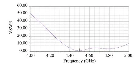
Fig.10.VSWR of high-resistance silicon substrate with air cavity.
Therefore,high-resistance silicon of the substrate and air cavity is essential.The charts of S11and voltage standing wave ratio(VSWR)are shown in Fig.9 and Fig.10.
When the frequency is 4.5 GHz,the S11and VSWR are minimums.Thus the frequency of 4.5 GHz is considered as the antenna’s resonant frequency.The minimums of S11and VSWR are –30.71 dB and 1.06.
According to Fig.11,the axial ratio value is 1.28 dB when Theta and Phi equal to 0°.For spherical coordinates,the angle Theta denotes the rotation from the x-axis towards the y-axis(positive poles,respectively),whereas Phi denotes the angular displacement from the x-y plane towards the positive pole of the z-axis.The antenna is approximately a circularly polarized antenna.It can receive mostly kinds of polarization of electromagnetic wave.
The E-plane and H-plane radiation patterns and the gain of the microstrip antenna array are separately shown in Fig.12 and Fig.13.
Compared with the low-resistant silicon and no air cavity antennas,the gain of the antenna with high-resistant silicon and air cavity has got a great improvement.The maximum of the gain is 8.09 dB.
4.Manufacture
The microstrip antenna array is manufactured by the MEMS technology and the precision machining technology.The main technologies are the etching technology,bonding technology,cutting technology,sputtering and plating technology,and packaging technology[12],as shown in Fig.14.
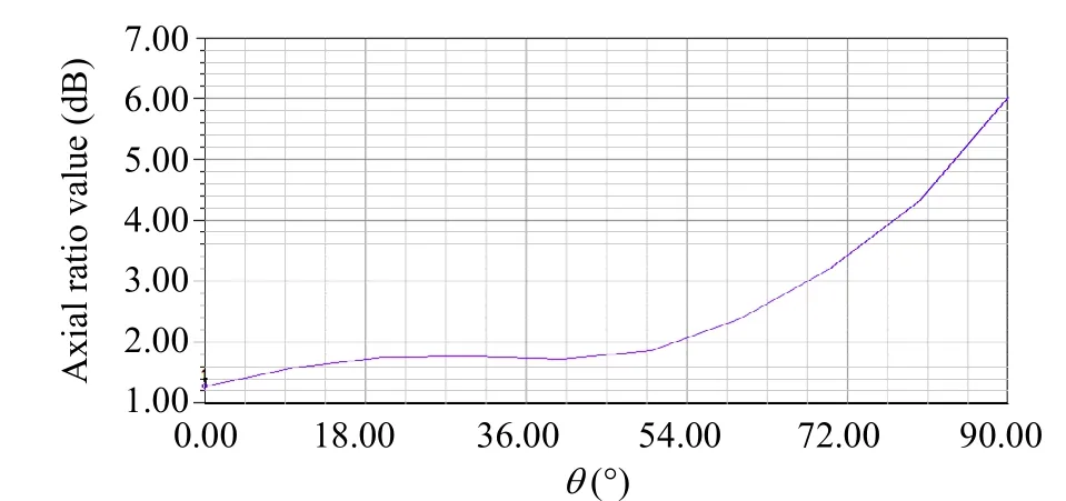
Fig.11.Axial ratio value of antenna array.

Fig.12.E-plane and H-plane radiation patterns of antenna array.

Fig.13.Gain of antenna array pattern.

Fig.14.Processes of manufacturing.
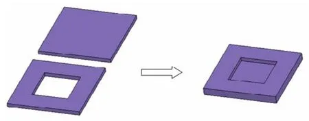
Fig.15.Process of etching air cavity.
In Fig.14,the most important technology is the cutting technology and etching technology.The material of high-resistant silicon has a high brittleness,and improper cutting method and cutting speed may cause the fragmentation of the antenna array.The better cutting method is multi-line cutting and the better cutting speed is 20 mm/min.
A new method is designed in the processing of the air cavity in the silicon substrate instead of directly using dry etching.There will be ±3 μm deviation by directly using dry etching and it will impact the electrical properties of the antenna.The new method is to etch through a 0.225 mm thick silicon by dry etching and then bonding to another 0.225 mm thick silicon.So the bottom surface flatness of the air cavity can be great guaranteed.The process of etching air cavity is shown in Fig.15.
5.Conclusions
In this paper,a MEMS C-band microstrip antenna array based on high-resistance silicon substrate is designed for the intelligent ammunition.The two elements of the patch are connected by an improved T-shaped power splitter.The microstrip antenna array is simulated by HFSS and its parameters are optimized.The best result is that S11equals to –30.71 dB and VSWR equals to 1.06.The value of axial ratio equals 1.28 dB.The total gain reaches to 8.098 dB.An improved dry etching method has been used in the antenna manufacture technology to reduce the processing error.The rate of finished products and the precision of cutting technology have been improved after studying of the cutting technology.
[1]Y.Liu,J.-P.Liu,and P.Li,“Designing a novel broadband microstrip antenna with capacitive reed,” in Proc.Int.Conf.of Cross Strait Quad-Regional Radio Science and Wireless Technology Conf.,Harbin,2011,pp.126–159.
[2]B.Z.Yang,“Design of monitoring analysis software for close-In weapon systems simulation,” in Proc.of 2010 Int.Conf.on Computer Application and System Modeling,Taiyuan,2010,pp.714–717.
[3]S.Sheng,“Impact of ammunition performance on weapon reliability & life cycle cost,” in Proc.of Reliability and Maintainability Symposium,Lake Buena Vista,2011,pp.1–5.
[4]J.Liu,“Application technology of MEMS inertial system,”in Proc.of 2010 Int.Conf.on Intelligent System Design and Engineering Application,Taiyuan,2010,pp.379–381.
[5]A.Olney,“Evolving MEMS qualification requirements,” in Proc.of Reliability Physics Symposium,Anaheim,2010,pp.224–230.
[6]R.R.Mansour,“RF MEMS devices,” in Proc.of 2003 Int.Conf.on MEMS,NANO and Smart Systems,Banff,ALberta,2003,pp.103–107.
[7]S.Ikram,“Design & implementation of a standard gain horn antenna for optimized gain and radiation pattern using MathCAD & HFSS,” in Proc.of the Second Int.Conf.on Electrical Engineering,Pakistan,2008,pp.1–5.
[8]Y.-D.Guo,X.-M.Liu,and Z.-G.Zhu,“Study of MEMS-based high-resistance silicon K-band planar array microstrip antenna,” in Proc.of 2010 Asia Pacific Conf.on Microelectronics and Electronics,Shanghai,2010,pp.368–371.
[9]Y.Koga and Y.Yoshida,“Cavity-backed MEMS patch antennas on double-layer silicon wafers,” in Proc.of IEEE Antennas and Propagation Society Int.Symposium,Chicago,2006,pp.3935–3938.
[10]J.-J.Yin and S.-L.Jia,Microwave Technology and Antenn-Electromagnetic Wave-Guide-Line and Radiation Engineering,Beijing:Electronics Industry Press,2005(in Chinese).
[11]D.M.Pozar,Microwave Engineering,3rd ed.,Beijing:Publishing House of Electronics Industry,2006,pp.271–275.
[12]R.Maeda,“Commercialization of MEMS and nano manufacturing,” in Proc.of the 6th Int.Conf.on Polymers and Adhesives in Microelectronics and Photonics,Odaiba,2007,pp.20–23.
 Journal of Electronic Science and Technology2013年1期
- Journal of Electronic Science and Technology的其它文章
- Low-Cost Embedded Controller for Complex Control Systems
- Data Hiding in DNA for Authentication of Plant Variety Rights
- An Image Authentication Method by Grouping Most Significant Bits
- A Steganography-Based Optical Image Encryption System Using RGB Channel Integration
- Rejection of Direct Blast Interference Based on Signal Phase-Matching Array Processing
- Investigation on Active and Reactive Combined Spot Price Integrated with Wind Farm