
OPTIMIZATION DESIGN METHOD FOR INPUT IMPEDANCE MATCHING NETWORK OF LOWNOISE AMPLIFIER
2011-10-08 12:10:04SunLingWuXianzhiAiXuesong
Sun Ling,Wu Xianzhi,Ai Xuesong
(Jiangsu Key Lab of ASIC Design,Nantong University,Nantong,226019,P.R.China)
INTRODUCTION
As illustrated in the "analog design octagon",the design of amplifiers is full of compromises[1],especially for a low noise amplifier(LNA),which is the first activestagein a receiver.LNA must operate at the samehigh frequency as carriers and must achieveimpedancematching,low noise figure(NF),high power gain,good linearity and so on.Therefore,it is necessary to trade these parameters each other during the LNA design,which also becomes its design difficulties.
According to the reported papers,many LNA circuits have been designed for different systems[2-5],and some optimization techniques have been considered.In Ref.[6],for example,a T-type input matching network was used to achieve a wideband input impedance matching.A novel noise optimization technique for inductively degenerated CMOS LNA was presented in Ref.[7].And in Ref.[8],a design method using mathematics optimization technology was proposed to obtain optimal transistor sizes and component values in input matching network and load network. For a certain LNA,a power-constrained optimization of simultaneous noise match and input match was given in Ref.[9].Different from those previously reported works,a convenient method based on Smith chart is advanced in this paper to obtain the optimal sourceimpedance for lower NF and the higher gain.
1 OPTIMAL NOISE MATCH AND POWER MATCH
As weall know,in the design of LNA,there exist an optimal source impedance to provide the lowest noise figure and an optimal source impedance to provide a maximum power gain.However,these two optimal source impedances are not equal,in other words,the optimal noise match and the power match cannot be achieved simultaneously.Therefore,a trade-off should be made between them.After a brief review of optimal noise match and optimal power match,a method for calculating the optimal source impedance is proposed to achieve the lowest noise figure and the maximum power gain under the constraint of input reflection coefficient S11.
1.1 Optimal noise match
A typical equivalent representation of a noisy two-port is shown in Fig.1,where Z s is the impedance of input source, Z L the load impedance,Z in the input impedance of the two port network,andare the equivalent input noise voltage and current respectively,v s is the voltage source andthe noise voltage source.The noise factor(F)in terms of F min and the source admittanceis given by[10]
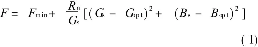
where F min is the minimum noise factor,R n the equivalent resistance,G s and B s are the conductance and the susceptance of the input source,while G opt and B opt the conductance and the susceptance of the input source at the minimum noise factor,respectively.The noise figure is the simple noise factor expressed in d B(NF=10log F).
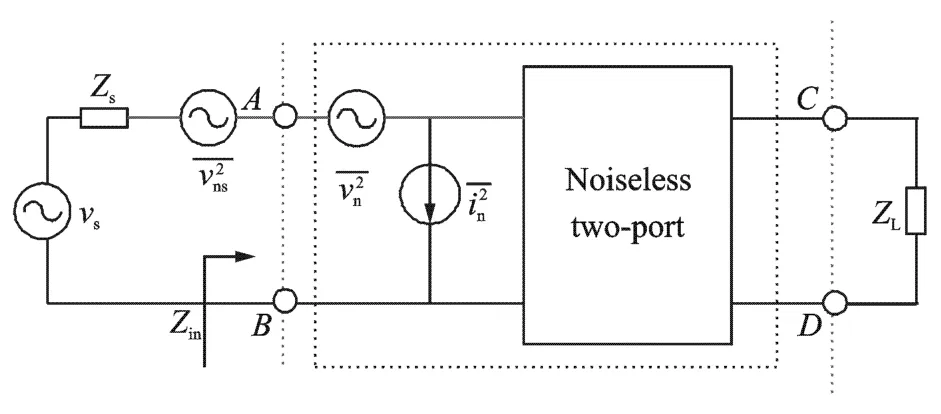
Fig.1 Equivalent representation of noisy two-port
The expression in Eq.(1)means that the contours of a constant noisefigure are circles centered about(G opt,B opt)on a Smith chart.Fig.2 shows an example of constant noise figure circles plotted on a Smith chart.Some important conclusions can be drawn as follows:The centers of all constant noise circles locate along a line drawn from the origin of the Smith chart to the point Y opt(Y opt=G opt+ j B opt).For the smaller noise figure,the center of noise figure circleis farther to the origin and the radius of the circle is smaller.When F=Fmin,the constant noise figure circle becomes a point and Y s=G opt+ j B opt.It means that if a matching network transfers the source impedance Y s to Yopt,the circuit is in the state of best noise match.It is called the optimal noise match,so Y op t is the optimal noise source admittance and Z opt the optimal noise sourceimpedance.
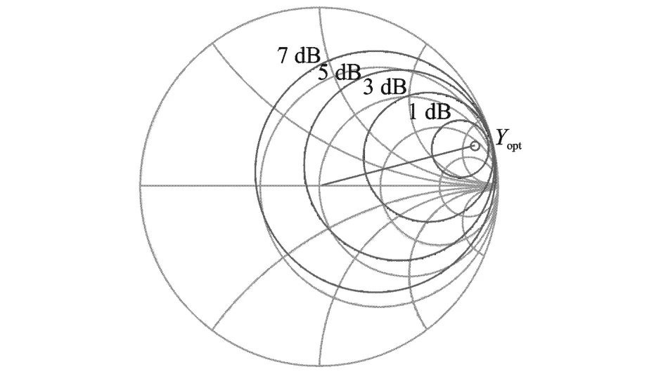
Fig.2 Bunch of constant noise figure circles
1.2 Optimal power match
The optimal power match for LNA means that the input impedance and the source impedance should be conjugate matched.In other words,the input matching network of LNA circuit should transform theinput impedance to 50Ω or transform 50Ωto the conjugate impedance of input.For there always exits a certain mismatch in real systems,the return loss,or S11,is used to specify this deviation.As shown in Fig.2,S11can be expressed in terms of impedance[11]as
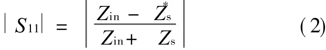
When Zs=,S11 has the minimum value and Z in*is called the optimal power sourceimpedance.Substituting Z in=R in+ j X in and Z s=R s+ j X s into Eq.(2),we have

so that
The expression in Eq.(4)denotes a set of constant S11 circles on the Smith chart,as shown in Fig.3,where Zs=Rs+ j X s is set as the variable.Similar to a constant noise figure circle and its conclusions,the centers of all constant S11 circles locate along a line drawn from the origin of the Smith chart to the point Z in*(Z in*=R inj X in).For the smaller S11,the center of the circle is farther to the origin and the radius of the circle is smaller.In other words,when the source impedance is closer to the optimal power source impedance Zin*,the S11is smaller.

Fig.3 Bunch of constant S11 circles
1.3 Trade-of f between optimal noise match and power match
As mentioned in previous section,the noise match or the power match can be achieved by moving source impedance to the optimal noise source impedance or the optimal power source impedance.Then,the remust bea suitablesource impedance to trade power match with noise match[12].At specified S11,a method for calculating this source impedance is introduced as follows.
According to the location of optimal noise source impedance on the Smith chart,there exist two cases.
(1)Optimal noise sourceimpedance is in the constant S11 circle.
As shown in Fig.4,when the optimal noise source impedance Z opt is in the constant S11 circle,which is the ideal condition,the LNA circuit can meet the S11 specification while achieving minimum noise figure.In this case,there is no need for compromise, just matching the source impedance to the optimal noise source impedance directly.
(2)Optimal noise source impedance is out of constant S11 circle.
As an example,assume that the required S11
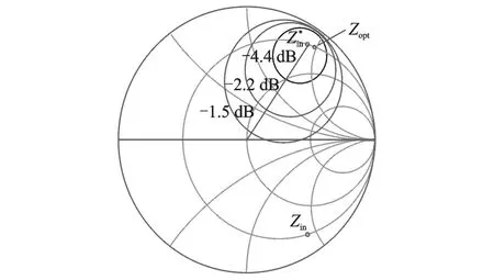
Fig.4 Z opt in constant S11 circle
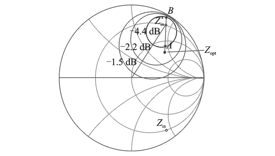
Fig.5 Z opt out of constant S11 circle
is- 4.4 d B and the optimal power source impedance is Z in*,while the optimal noise source impedance Z op tis out of-4.4 d Bcircle,as shown in Fig.5.By drawing a straight line between Z in*and Z op t,there exist two points,denoted by A and B,where the lineintersects thecontour of S11 circle with the constant value-4.4 d B.As we can see,point A is closer to Z op t,soit is the point of lowest noise figure at this S11 circle.By moving source impedance to point A,the optimal noise match is achieved at this specified S11.A detailed calculation process is shown as follows.
Theinput impedance

Theoptimal power source impedance

Theoptimal noisesource impedance

Thesource impedance

The linear equation connected Z in*and Z opt

The circle equation of constant S11
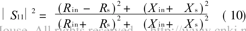
The distance from the cross point to the optimal noise source impedance is

From Eqs.(9,10),the impedances at point A(ZA=RA+ j XA)and point B(ZB=RB+ j XB)can be solved respectively . Then , using Eq.(11),the distance can be calculated.The point which has the closer distance is the desired solution.With the help of mathematical tools,the calculate process is easier and faster.Mathcad,one of engineering calculation software,is used in the design.
2 DESIGN EXAMPLE
Based on the Chart 0.35-μm CMOSprocess,a cascode LNA circuit without input/output matching network is designed to verify the method.The total die area is 368μm× 554μm.Fig.6 shows its schematic and micrograph with test probes.And its on-chip measured S-parameters are shown in Fig.7.

Fig.6 Cascode LNA without input/output matching network

Fig.7 Measured S-parameters of LNA without matching network
2.1 Calculation of required optimal source impedance
In this work,the designed LNA circuit is aimed at UHF RFID systems,and the centre operation frequency is 922.5 MHz.After an SP simulation in Cadence Spectre at 922.5 MHz,we have:
The input impedance

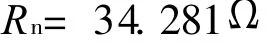
The equivalent resistance
The optimal conductance of input source
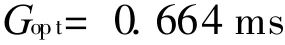
The optimal susceptance of input source

The minimum noise figure

The noise factor

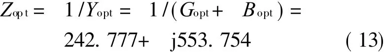
Therefore, the optimal power and noise sourceimpedances of this designed LNA at 922.5 MHz are

Assuming that the specified S11< -10 d B,from Eqs.(9,10),we obtain ZA=53.975+j216.232 and ZB=102.921+ j304.206.Further,from Eq.(11),we have
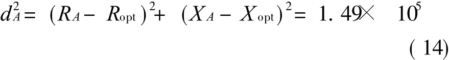

As wecan see,d2B<d2A,the cross point ZB is the required optimal sourceimpedance.The noise figures and the corresponding S11 at different source impedances aresimulated in Cadence Spectre and the results are listed in Table 1.
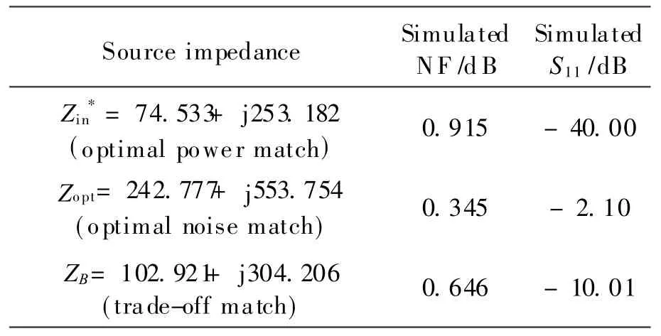
Table 1 NF and S11 at dif ferent source impedances
2.2 Design of input impedance matching network
According to thecalculated results,theinput impedance matching process is to pull ZB to 50Ω or to pull 50Ωto ZB.There are many different topologies of matching network,the T-type is chosen in this design and a matching sketch is shown in Fig.8.

Fig.8 Sketch of input impedance matching network
Based on the on-chip measured S-parameters of LNA without matching network(Fig.7)and the model parameters of passive components(inductors and capacitors)from Murata Manufacturing Co.Ltd,the input and output impedance matching networks are accomplished in ADSand the experimental results are shown in Figs.9,10.We can see that at 922.5 MHz,NF is 0.656 d B(point m2)and S11 is-13.094 d B(point m1).Here,the value of NFis 0.01 d Bhigher than the one listed in Table 1 while S11 is 3 d Blower.
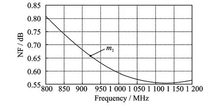
Fig.9 Curve of noise figure
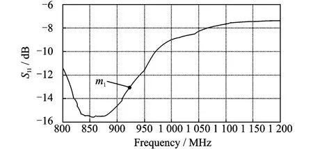
Fig.10 Curve of S11
3 CONCLUSION
A clearer and more straightforward understanding of optimal noise match and optimal power match is presented.With the help of Smith chart,the detailed calculation of desired source impedance is advanced for trade-off match at specified S11.Based on Chart 0.35-μm CMOS process,LNA for UHF RFID systems is designed and its simulation and experimental results are analyzed.Finally the design example proves the feasibility of the calculation method.
[1] Razavi B.Design of analog CMOS integrated circuits[M].New York:McGraw-Hill,2001.
[2] Cai Li,Fu Zhongqian,Huang Lu.A low power high gain UWB LNA in 0.18-μm CMOS[J].Journal of Semiconductors,2009,30(11):115004.
[3] Chang Chieh-Pin,Chen Ja-Hao,Wang Yeong-Her.A fully integrated 5 GHz low-voltage LNA using forward body bias technology[J].IEEE Microwave and Wireless Components Letters,2009,19(3):176-178.
[4] Xu Leijun,Wang Zhigong,Li Qin,et al.Design of a 40-GHz LNA in 0.13-μm SiGe BiCMOS[J].Journal of Semiconductors,2009,30(5):055005.
[5] Lee JH,Chen CC,Lin Y S.3.7 mW 24 GHz LNA with 10.1 d Bgain and 4.5 d B NFin 0.18-μm CMOS technology[J].Electronics Letters,2010,46(19):1310-1312.
[6] Wang C H,Chiu Y T,Lin Y S.3.1 d B NF 20-29 GHz CMOSUWB LNA using a T-match input network[J].Electronics Letters,2010,46(19):1312-1313.
[7] Geng Zhiqing,Wang Haiyong,Wu Nanjian.Anovel noise optimization technique for inductively degenerated CMOS LNA[J].Journal of Semiconductors,2009,30(10):105015.
[8] Liu Mengmeng,Zhang Sheng,Wang Shuo,et al.An optimization design methodology for CMOS UWB LNA[J].Acta Electronical Sinica,2009,37(5):1082-1086.(in Chinese)
[9] Mao Xiaofeng, Lan Jialong, Huang Chaogang.CMOS narrow-band LNA design optimization with low-power dissipation[J].Semiconductor Technology,2007,32(5):417-421.
[10]Ludwig R,Bretchko P.RF circuit design: Theory and applications[M].Beijing:Science Press,2002.
[11]Kurokawa K.Power waves and the scattering matrix[J].IEEE Transactions on Microwave Theory and Techniques,1965,13(2):194-202.
[12]Circult Sage.Optimal sourceimpedance to trade-off power and noise and to achieve a desired S11[EB/OL].http://www.circuitsage.com/lnapa/powernoise.pdf,2011-01.
 Transactions of Nanjing University of Aeronautics and Astronautics2011年4期
- Transactions of Nanjing University of Aeronautics and Astronautics的其它文章
- VOLUMETRIC-SWEPT DISPLAY SYSTEM BASED ON HELIX ROTATING SCREEN AND DMD
- MODELING AND SIMULATION OF E1784K MUTATION AND SODIUM IONIC CHANNEL DISEASES
- DIRECT SELF-REPAIRING CONTROL FOR HELICOPTER VIA QUANTUM CONTROL AND ADAPTIVE COMPENSATOR
- CHARACTERISTICSOF FAN STALLING BASED ON CORRELATED DIMENSIONS
- HYBRID SCHEME FOR COMPRESSIBLE TURBULENT FLOW AROUND CURVED SURFACE BODY
- PRE-CORROSION FATIGUE NOTCH FACTOR