通過構(gòu)象誘導(dǎo)電感耦合機制光可逆調(diào)控有機場效應(yīng)晶體管的性能
2010-12-12 02:44:14王振興惠靜姝郭雪峰
物理化學(xué)學(xué)報 2010年7期
關(guān)鍵詞:實驗室
申 茜 甘 霖 劉 松 曹 陽 王振興 惠靜姝 郭雪峰
(北京大學(xué)化學(xué)與分子工程學(xué)院,分子動態(tài)與穩(wěn)態(tài)結(jié)構(gòu)國家重點實驗室,北京分子科學(xué)國家實驗室,北京 100871)
Over the past decade great progress has been made on organic thin-film transistors(OTFTs)with impressive achievements in improving carrier mobilities that are now comparable to those of amorphous silicon thin-film transistors[1-4].For the practical application of OTFTs in low-cost,solution-processed/printed electronics-based sensors and displays,the next step of crucial importance is to install functionality into a simple OTFT such that the device is capable of converting an external stimulus to an easily detectable electrical signal.In fact,OTFTs have been envisioned as an ideal platform for developing robust,inexpensive chemical or biological sensors[5-17]because of their inherent advantages such as easy availability,compatibility with flexible, large-area substrates and highly tunable sensitivity.For example, recent work has shown that a proper selection of the semiconductors and gate dielectric materials can lead to reliable OTFT operations in the aqueous media that are required for biosensing[9,18]. The sensing mechanism of these sorption-based sensors has been attributed to the analytes′diffusion into grain boundaries in thin films that cause either trapping or doping of charge carriers.This mechanism provides sensitive detection for chemical and biological species,but the physically damaging interaction between semiconductors and analytes,and the difficulty of removing analytes could lead to serious problems of device stability and reversibility,being one of the major obstacles to the practical application of OTFTs in sensing.There is a pressing need to develop a noninvasive methodology of modulating the density of charge carriers flowing through the active semiconductor layers;this should be fully reversible and it should leave the semiconductors essentially untouched.
Here,we detail a smart system,by which OTFTs performance can be reversibly fine-tuned by lights with different wavelengths.This study builds on our recent work in which we demonstrated that photochromic spiropyrans can be assembled to the surfaces of single-walled carbon nanotubes through molecular self-assembly[19]and to pentacene thin films through rubber stamping[20]to make photosensitive devices.In both cases UV and visible light irradiation can switch the device conductance back-and-forth between two distinct states by either reversible, conformation-induced doping or electrostatic effects.In the current case,we use a hybrid gate dielectric,which is composed of a buffer polymer carrier,polymethyl methacrylate(PMMA,MW= 4.95×10⁵),and a photoresponsive molecule driver,photochromic spiropyran(SP).When the SP molecules undergo the reversible photoisomerization[21-22],we are able to regulate the capacitance of the gate dielectric,and this leads to the reversible photomodulation of the device characteristics of OTFTs in a noninvasive manner.
1 Results and discussion
A typical top-contact,bottom-gate OTFT device configuration was used in this study(Fig.1).The dielectric we used was a hybrid polymer bilayer(PMMA+SP,300 nm,top)/(SiO2,100 nm, bottom).We used the corresponding thin films without the SP additive as control dielectrics.To maximize the switching behavior of functionalized OTFTs,we used the hybrid dielectric with SP saturation concentration of~0.07 mol·L-1.We chosed the hybrid PMMA dielectrics with 300-nm thickness as a representative because we found that this thickness of hybrid dielectrics gave the best photoresponsivities.Pentacene was chosen as the model organic semiconductor because of its high mobility and the importance of this material for incorporation into electronic circuitry[1-3].
Tapping-mode atomic force microscopy(AFM)images obtained from the hybrid gate dielectric surfaces demonstrated smooth surface morphologies(maximum root mean square roughness~0.3 nm)(Fig.2(a)).UV/visible absorption studies showed that SP molecules in thin films of the hybrid gate dielectric were able to reversibly switch back-and-forth between the neutral closed form(SP-closed)and the charge-separated,colored open form(SP-open)under UV and visible light irradiation(Fig.3(a)). This indicates that PMMA can serve as a good matrix for SP molecules.It can provide buffering space for SP′s conformational changes.After 40-nm pentacene deposition via thermal evaporation,we obtained large pentacene crystal grains with terraces (step heights about 1.5 nm)as demonstrated by AFM(Fig.2(b, c)).X-ray diffraction measurements also demonstrated the formation of highly crystal-quality pentacene thin films on top of the dielectric(Fig.3(b)).These results are important to achieve optimal OTFT performance.After deposition of top Au chargeinjecting and charge-extracting source and drain electrodes through thermal evaporation under vacuum,the desired transistors were obtained.The channel length of the devices was 60 μm and the width was 2000 μm.The capacitance of the hybrid dielectric films was measured on the sandwich electrode structures with gold pads(0.9 mm2)using a Karl Suss probe station equipped with a digital capacitance meter(Agilent 4294A).The transistor properties were characterized with the same probe station and a semiconducting parameter analyzer(Agilent 4155C). Carrier mobilities(μ)were calculated in the saturation regime by the standard method:ID=WCiμ(VG-VT)2/(2L),where IDis the source-drain saturation current,W is the channel width,L is the channel length,Ciis the gate dielectric capacitance(per area),VGis the gate voltage,and VTis the threshold voltage.Light irradiations were performed with a handheld UV lamp(~100 μW·cm-2, λ=365 nm)and with a 150 W Halogen incandescent lamp(Imax:~30 mW·cm-2,λ>520 nm).To avoid the heating effect during irradiation,visible light was focused and guided by a long optical fiber to the probe station.To aid in the analysis of the results, we intend to regulate the intensity of visible light that makes the photocurrents of the devices under visible irradiation equivalent to those induced by UV irradiation.By doing this,we can record the time trace of the drain currents of the devices without obvious current jumps when UV and visible lights are switched.All of the measurements were performed in the same condition and at the same temperature.OTFTs fabricated with 300 nm hybrid polymer/100 nm SiO2bilayer dielectrics achieved a mobility of as high as 0.13 cm2·V-1·s-1(Fig.4).
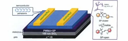
Fig.1 Schematic representation of the top-contact,bottom-gate OTFT structure and the material components

Fig.2 AFM images of the sample surfaces(a)representative tapping-mode AFM images(5.0 μm×5.0 μm)obtained from the hybrid gate dielectric surfaces(PMMA thickness:300 nm and SP concentration:0.07 mol·L-1),(b)representative tapping-mode AFM images(5.0 μm×5.0 μm)of surface morphologies of 40-nm pentacene thin films grown on the hybrid gate dielectric,(c)representative tapping-mode AFM images(1.5 μm×1.5 μm)of pentacene thin film surfaces

Fig.3 (a)UV/visible absorption spectra of a PMMA-spiropyran thin film(thickness:300 nm and SP concentration of 0.07 mol· L-1)on a quartz substrate under UV light irradiation,(b)X-ray diffraction spectrum of 40-nm pentacene thin films on a hybrid gate dielectric with film thickness of 300 nm and SP concentration of 0.07 mol·L-1

Fig.4 Representative output and transfer characteristics of devices on silicon wafer substrates with a hybrid polymer (PMMA+SP,top)/SiO2(100 nm,bottom)bilayer dielectricSP concentration is 0.07 mol·L-1.PMMA thickness is 300 nm.Ciis~3.6 nF.The channel length of the devices is 60 μm and the width is 2000 μm.
We tested the photoswitching characteristics of the devices and found that large and reversible changes in drain current occurred in these SP-functionalized OTFTs when SP isomerized between SP-closed and SP-open forms(Fig.5(a-e)).As shown in Fig.5(a),after~270 s of UV irradiation,the initial(low)conductance state of the device(black curve,Ron:~1.5×10¹⁰Ω at~30 V source/drain bias and~20 V gate bias)was converted into a much higher conductance state(red curve,Ron:~7.9×10⁹Ω).After further visible light irradiation for~24 min(green curve in Fig.5(a)),the drain current of the device was essentially restored to its original value.The back-and-forth photoswitching effect is rathergradual in time.Fig.5(b,c)show the time-evolution ofthe current-voltage curves during UV and visible light illumination, respectively.The drain current sharply increased at the beginning of UV irradiation and was saturated after~270 s of exposure when SP molecules reached the equilibrium of conformational transformation(Fig.5(b)).On the contrary,after the highconductance state was established and irradiation with visible light began,the drain current of the same device sharply decreased initially and then slowly attenuated,completing the decrease after~24 min illumination(Fig.5(c)).The similarity between the reversible photoswitching of the electrical conductivity of the functionalized devices and the reversible photoisomerization of SP molecules suggests that the photoswitching process of SP molecules is responsible for the changes in device characteristics of pentacene OTFTs.To gather kinetic data for the photoswitching process,we monitored the drain current as a function of time (VD=-30 V,VG=-20 V)asthe irradiation was toggled between UV and visible wavelengths.To clearly demonstrate the photoswitching process and mechanism discussed below,we do not show the slow back-conversion process of the devices in the dark after UV irradiation due to the slow transformation of SP from SP-open to SP-closed.Fig.5(d)shows one full switching cycle of the time-dependent behavior of the same device;this behavior is consistent with the results from Fig.5(b,c).A sudden current jump was also observed at the moment of turning on UV light generally due to the photoexcited state of organic semiconductors as proved by control experiments in Fig.6(c).In order to demonstrate the reversibility of the switching,we used shorter irradiation time.As shown in Fig.5(e),all the functionalized OTFTs are quite stable and can switch at least 50 times in ambient atmosphere without obvious degradation.The kinetics of each process can be fit with a single-exponential.Based on the data in Fig.5(e),the overall rate contants in different parts were calculated,KUV:~(1.6±0.2)×10-2s-1and Kvisible:~(0.7±0.1)×10-2s-1. These kinetic results for the photoswitching process are very similar to or even faster than those we observed in our previous work[19-20],which supports our suggestion(see above)that PMMA thin films serve as an effective solid matrix in which the SP molecules can isomerize.To aid in the analysis of these results, we performed control experiments in which we measured the photoresponse ofa pentacene device having the same PMMA/SiO2bilayer dielectric but lacking the spiropyran.Fig.6 shows the drain current characteristics of such a device as a function of time under the same measurement conditions.During irradiation with either UV or visible light,we consistently observed the slow decrease in drain current,probably resulting from problems associated with the device stability.From the trace in Fig.6,the overall rate constants for each part were obtained,both KUVand Kvisibleare~(5.0±0.1)×10-4s-1.In comparison with those in functionalized devices,two significant differences should be pointed out.One is that the rate constants of the device in Fig.5(e)under UV and visible light irradiation are two orders of magnitude larger than those obtained from the control device in Fig.6 under the same conditions.The other significant difference is that the photoswitching effect under UV illumination in functionalized devices is opposite to that in the control devices.It is quite clear that the photoisomerization of SP molecules is responsible for the switching effect in device characteristics.

Fig.5 (a)A representative photoswitching cycle in a 40 nm pentacene thin film transistor with dielectric thickness of 300 nm and SP concentration of 0.07 mol·L-1;(b,c)the gradual conversion between low and high conductance states when the currentvoltage curves are taken every 30 s for UV illumination and every 2 min for visible light illumination,respectively;(d)one full switching cycle of the time-dependent behavior of the same device;(e)time trace of the drain current for the same device showing the reversible photoswitching events under irradiation of UV light(365 nm)and visible light(λ>520 nm)The bias between source and drain electrodes is-30 V,and the gate bias is-20 V.

Fig.6 (a)output and(b)transfer characteristics of a control device on silicon wafer substrates with a polymer (300 nm PMMA,top)/SiO2(100 nm,bottom)bilayer dielectric,(c)time trace of the drain current for the same device under irradiation of UV light(365 nm)and visible light(λ>520 nm)The bias between source and drain electrodes is-30 V,and the gate bias is~20 V.Ciis-6.1 nF.The channel length of the devices is 60 μm and the width is 2000 μm.The calculated mobility is~0.5 cm2·V-1·s-1.
Theoretical discussion[20]has suggested that the photoisomerization of photochromic molecules will significantly change their dipole moment(Pmol).We performed density functional theory calculations and the result shows that the electric dipole moment of the open form SP is 46.4×10⁻³⁰C·m,more than two times of the dipole moment of the closed form(21.3×10⁻³⁰C·m). In our previous work we showed that this photoinduced electrostatic environment should act as a local negative gate voltage that can modulate the transistor conductance by controlling the carrier density in devices[19-20].We hypothesized that the SP photoisomerization could initiate the reversible changes in capacitance of the hybrid gate dielectric and thus modulate the electrical conductivity of the devices.
To prove this hypothesis,we tested the electrical characteristics of ITO/hybrid dielectrics(PMMA+SP)/Au capacitors.In order to avoid the shading of the UV and visible light,we irradiated the hybrid material from the bottom of ITO transparent electrodes.Fig.7(a,b)show the time-dependent evolution of the capacitance curves of a hybrid polymer dielectric at SP concentration of 0.07 mol·L-1and PMMA thickness of 300 nm.From the time course of the device capacitance,we can see that the capacitance increased sharply at the beginning of UV irradiation and then saturated after~260 s of exposure,further visible light irradiation can return it to its original value.The whole process is quite reversible.We show 4 representative full switching cycles of the same device by taking the data at 100 kHz frequency(Fig. 7(c)).In order to rule out other potential artifacts we performed control experiments.In the control device we used only PMMA thin films with the same thickness as the dielectric without the SP additive.Under UV or visible light irradiation,there was only negligible increases in capacitance(Fig.8),which may be due to the slight effect of the dissociative photoexcitation of C—C or C—H bonds of polymer PMMA on capacitance[23-24].From the results we may conclude that the photoisomerization of the SP molecules are responsible for the photoswitching of the capacitance in devices.Since SP photoisomerization can induce a big change in dipole moment of individual molecules and SP molecules serve as the key component of the gate dielectric,it is reasonable that this dipole change could initiate a collective change in dielectric constant of the gate dielectric,thus leading to the reversible photomodulation of the capacitance of the gate dielectric and then the carrier density at the semiconductor/dielectric interface.Consequently,it is not surprising that SP photoisomerization can realize the reversible photoregulation of the electrical conductivity of the devices as demonstrated experimentally through a novel mechanism:conformation-induced capacitive coupling.Another important feature which should be mentioned is that all of the conformational changes happen within the gate dielectric layer driven by the most convenient and noninvasive tool of lights without any damage of the semiconductors,making the functioning devices very stable.

Fig.7 Demonstration of the switching mechanism(a)and(b)Time course of the capacitance of a hybrid polymer dielectric on ITO glass substrates upon UV and visible light irradiation. SP concentration is 0.07 mol·L-1.PMMA thickness is 300 nm.The capacitance-frequency curves are taken every 20 s for UV illumination and every 2 min for visible light illumination.(c)The representative 4 full switching cycles of the same device by taking the data at 100 KHz frequency.

Fig.8 Time-evolution of the capacitance curves of control dielectric absent of SP molecules on ITO glass substrates under UV and visible light irradiationPMMA thickness is 300 nm.The capacitance-frequency curves are taken every 20 s for UV illumination(a)and every 2 min for visible light illumination(b).
2 Conclusions
In this study,we detailed a smart system,in which the OTFT performance can be fine-tuned by UV and visible light irradiation using a hybrid gate dielectric composed of a photochromic molecule SP and a polymer buffer PMMA.When the SP molecules underwent their documented reversible photoisomerization,the reversible changes in capacitance of the hybrid gate dielectric was observed due to the changes of the electric dipole moment of the molecules,thus leading to reversible photomodulation of the electrical conductivity of the devices.Since SP photoisomerizations happen only within the gate dielectric layer and the most convenient and noninvasive tool of lights is used,organic semiconductors are essentially untouched without any damage,making the devices very stable.This concept of conformation-induced capacitive coupling offers attractive new prospects for the development of functional molecular by utilizing other stimuli-responsive molecular materials.
1 Murphy,A.R.;Frechet,J.M.J.Chem.Rev.,2007,107:1066
2 Kagan,C.R.;Andry,P.Thin-film transistors.New York:Dekker, 2003
3 Zaumseil,J.;Sirringhaus,H.Chem.Rev.,2007,107:1296
4 Reese,C.;Bao,Z.Mater.Today,2007,10:20
5 Janata,J.;Josowicz,M.Nat.Mater.,2003,2:19
6 Katz,H.E.Electroanalysis,2004,16:1837
7 Locklin,J.;Roberts,M.;Mannsfeld,S.;Bao,Z.Polym.Rev.,2006, 46:79
8 Mabeck,J.T.;Malliaras,G.G.Anal.Bioanal.Chem.,2006,384: 343
9 Wang,L.;Fine,D.;Sharma,D.;Torsi,L.;Dodabalapur,A.Anal. Bioanal.Chem.,2006,384:310
10 Huang,J.;Miragliotta,J.;Becknell,A.;Katz,H.E.J.Am.Chem. Soc.,2007,129:9366
11 Torsi,L.;Farinola,G.M.;Marinelli,F.Nat.Mater.,2008,7:412
12 Crone,B.;Dodabalapur,A.;Gelperin,A.Appl.Phys.Lett.,2001, 78:2229
13 Feldman,A.K.;Steigerwald,M.K.;Guo,X.;Nuckolls,C.Acc. Chem.Res.,2008,41:1731
14 Torsi,L.;Lovinger,A.J.;Crone,B.J.Phys.Chem.B,2002,106: 12563
15 Torsi,L.;Dodabalapur,A.;Sabbatini,L.;Zambonin,P.G.Sens. Actuator B-Chem.,2000,67:312
16 Guo,X.;Xiao,S.;Myers,M.;Miao,Q.;Steigerwald,M.L.; Nuckolls,C.Proc.Natl.Acad.Sci.U.S.A.,2009,106:691
17 Someya,T.;Yusaku,K.;Sekitani,T.Proc.Natl.Acad.Sci.U.S. A.,2005,102:12321
18 Roberts,M.E.;Mannsfeld,S.C.B.;Bao,Z.Proc.Natl.Acad.Sci. U.S.A.,2008,105:12134
19 Guo,X.;Huang,L.;O′Brien,S.;Kim,P.;Nuckolls,C.J.Am. Chem.Soc.,2005,127:15045
20 Shen,Q.;Steigerwald,M.L.;Guo,X.J.Phys.Chem.C,2009, 113:10807
21 Berkovic,G.;Krongauz,V.;Weiss,V.Chem.Rev.,2000,100, 1741
22 Guo,X.;Zhang,D.;Yu,G.;Wan,M.;Li,J.;Liu,Y.;Zhu,D.Adv. Mater.,2004,16:636
23 Benson,N.;Schidleja,M.;Melzer,C.;Schmechel,R.;von Seggern,H.Appl.Phys.Lett.,2006,89:182105
24 Hollander,A.;Klemberg-Sapieha,J.E.;Wertheimer,M.R. Macromolecules,1994,27:2893
猜你喜歡
電子競技(2020年8期)2020-12-23 04:09:40
電子競技(2020年7期)2020-10-12 10:45:48
電子競技(2020年5期)2020-08-10 08:43:10
電子競技(2020年4期)2020-07-13 09:18:06
電子競技(2020年2期)2020-04-14 04:40:38
電子競技(2020年11期)2020-02-07 02:49:36
電子競技(2020年9期)2020-01-11 01:06:21
電子競技(2020年10期)2020-01-11 01:06:06
電子競技(2019年22期)2019-03-07 05:17:26
電子競技(2019年21期)2019-02-24 06:55:52