
簡易方法制備交叉碳納米管-石墨烯異質(zhì)結(jié)
2010-12-12 02:41:28李丹娜陽申王振興郭雪峰
物理化學(xué)學(xué)報 2010年4期
甘 霖 劉 松 李丹娜 谷 航 曹 陽申 茜 王振興 王 青 郭雪峰
(北京大學(xué)化學(xué)與分子工程學(xué)院,分子動態(tài)與穩(wěn)態(tài)結(jié)構(gòu)國家重點實驗室,北京分子科學(xué)國家實驗室,北京 100871)
The engineering of molecular devices relies on the control and exploration of the electronic properties of the junctions. These properties include the intrinsic electronic device functions as well as the ability of the molecules to interact with the electrodes.Among these functions,rectification behavior is one of the most exciting device functions,which was first envisioned by Aviram and Ratner[1].The Aviram-Ratner molecular diode consists of a donor and an acceptor separated with a σ bridge in which the forward current is from the acceptor to the donor.To date,most experimental studies of molecular diodes have been carried out using Langmuir-Blodgett films[2-3]and self-assembled monolayers(SAMs)[4-6].However,the study of the diode behaviors in these molecular junctions is significantly limited due to the requirement of sophisticated and time-consuming device fabrication and the unavailability of the molecules with desired structures.
Another efficient approach to realize the rectification behaviors at the molecular level is to form T-or Y-shaped heterojunctions between different nanomaterials.In the past decade,much effort has been made to create nano-heterojunctions between nanotubes(NTs)and nanowires(NWs)because they could provide building blocks for nanoelectronics and nanophotonics[7-9]. Although several types of nano-heterojunctions between nanotubes and nanowires have been made[8-13],the key question of the fabrication of the nano-heterojunctions remained a significant challenge.This is due to the difficulty of direct growth of T-or Y-shaped heterojunctions.In this work,we report a facile technique for producing a large number of crossed nanotubegraphene heterojunctions through a nondestructive polymethyl methacrylate(PMMA)-mediated nanotransfer printing approach[14-15]and selective oxygen plasma etching.Then through only one-step electron beam lithography,we can easily fabricate the corresponding nanodevices.
Single-walled carbon nanotubes(SWNTs)[16]and single-layer graphene(SLG)[17],two star molecules of carbon nanomaterials, have been proposed as the ideal systems for nanoelectronics and molecular electronics in both academic and industrial communities[18-22].Nanojunctions consisting of two crossed SWNTs were fabricated to form two-and three-terminal devices,which showed a rectifying Schottky barrier[23].However,a question remains: what will happen when individual SWNTs are joined with SLG to form multi-terminal devices and,ultimately,complex circuits?To answer this question,in this study we focus on the technical development of building SWNT-SLG heterojunctions formed by graphene that lie across nanotubes on silicon wafer substrates(Fig.1).
1 Results and discussion
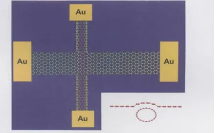
Fig.1 Schematic structure of the crossed SWNT-SLG heterojunctionsInset shows the assumption that deformations in both SWNT and SLG could happen at the junction due to their interaction with SiO2substrates.
A schematic procedure for fabricating the SWNT-SLG heterojunctions is given in Fig.2.Although the final SWNT-SLG heterojunctions are obtained through 9 steps,each step is quite simple without either traditional photolithography or complicated electron beam lithography.Within one or two days,one could use this facile procedure to mass produce SWNT-SLG heterojunctions.Firstly we synthesize SLG through a chemical vapor deposition process(CVD).Currently,several promising synthesis methods have been developed to grow SLG.These include epitaxial graphene on SiC[24-25],graphene oxide reduction[26-27],direct growth out of thin nickel film[28-29],and most recently on copper foils[30].Among these methods,the latest copper foil-based synthesis is the most effective in producing large continuous SLGs with promising electrical properties.In our procedure,we use 25 μm thick copper films(Alfa Aesar)to grow our SLG. The basic mechanism is similar to that recently reported in Ref. [30].Before graphene growth,Cu films were immersed in acetic acid at 40℃for 15 min in order to remove most of the copper oxide.We found that this is an important pretreatment because removal of the copper oxide prior to growth improves the quality of the copper film and thus the quality of SLG.A typical growth process is listed below.A quartz substrate with the Cu film was loaded into the furnace.Then the system was evacuated and heated to 1000℃under a 10 cm3·min-1flow of H2at a pressure of about 50 Pa.After stabilizing the Cu film at the desired temperature,we introduced 1.1 cm3·min-1of CH4for 5-10 min at a pressure of about 60 Pa.After the growth the substrates were then cooled down to room temperature for the next transfer step.Fig.3(a)shows a contrast-enhanced optical image of a typical sample substrate after graphene growth.We found that graphene was continuous across the visible Cu grains as demonstrated below.Fig.3(b)presents a Raman spectrum that is representative of the grown graphene.A single symmetric 2D peak (full width at half-maximum ca 34 cm-1),a small G/2D ratio,and a negligible D peak are observed,which strongly suggest that the graphene is a single layer and the quality of the sheet is not significantly affected by the visible features of the Cu film[30].
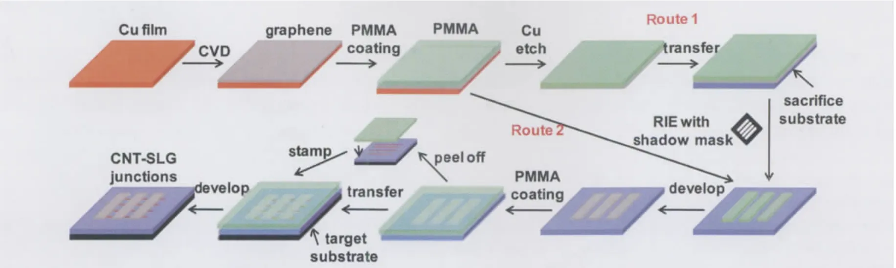
Fig.2 Schematic representation of the fabrication procedure to form crossed nanotube-graphene heterojunctions
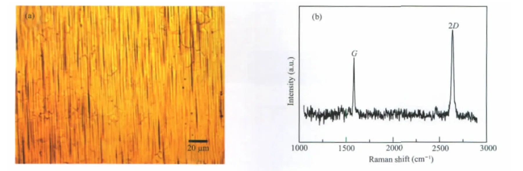
Fig.3 (a)A contrast-enhanced optical image of a typical sample substrate after graphene growth, (b)a representative Raman spectrum of the grown graphene

Fig.4 (a)An optical image of large-area graphenes after PMMA-mediated nanotransfer process,(b)an optical image of graphene sheet array after oxygen plasma etching and the zoomed-in image of the part labeled by a red square, (c)Raman spectra obtained from the marked spots with the corresponding colored circles
After graphene growth,polymer PMMA with 300 nm thickness was spin coated on the Cu films.The whole samples were then immersed into a continually refreshed saturated solution of iron nitrate for an enough long time to remove the Cu substrates. The resultant transparent sheet floating in the aqueous solution was transferred to a sacrifice silicon substrate.To demonstrate the efficiency of the PMMA-mediated transfer technique,we simply tested the quality of graphene after removing PMMA in a boiling acetone solution.As shown in Fig.4(a),this method allows us to transfer large-area continuous high-quality graphenes with only small residues to any kinds of substrates as confirmed by Raman measurements(see below).To form graphene sheets, we directly applied an oxygen plasma etching process(oxygen: 19 cm3·min-1,pressure:35 Pa,power:50 W)for 2.5 min without removing PMMA thin films after the transfer step to etch away the unprotected graphene beneath the exposed PMMA through a shadow mask.Then after removing the remaining PMMA in a boiling acetone solution,graphene sheets with desired patterns were obtained.Fig.4(b)shows an optical image of the resulting sheet array with ca 100 μm width separated by ca 500 μm.In principle,graphene microarrays with any kinds of patterns could be easily obtained through this flexible process,depending on the design of the shadow mask.A zoomed-in optical image of one part is also shown in Fig.4(b).This contrast-enhanced image confirms that the surface of SLG sheets is very clean without obvious damages and any visible residues on top of them.To further evaluate the quality and uniformity of the transferred graphenes,we used Raman spectroscopy to characterize them. Fig.4(c)showsthe correspondingRaman spectra fromthe marked circles with different colors in Fig.4(b).Surprisingly,the resulting graphene sheets show the uniform Raman signature over large areas and remain the same original quality as shown in Fig. 3(b).Based on the Raman analysis,we estimated the SLG coverage to be a minimum of 93%[30].The Raman measurements as well as the optical characterization demonstrate that this nanotransfer and oxygen plasma etching process is useful for making large-area high-quality graphene microdevices in a nondestructive manner.We found that the sequential transfer and oxygen plasma etching process is important.If the oxygen plasma etching is straightly applied on the Cu films without the transfer step as shown in Fig.2(Route 2),extensive damages of the graphene sheets can occur probably due to the fragility of Cu films.
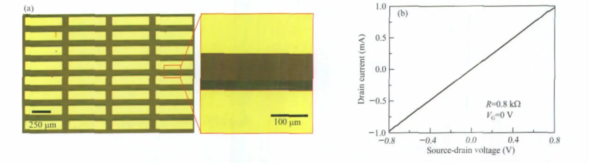
Fig.5 (a)Schematic representation of the SLG device array and the enlarged optical image of a representative device, (b)a representative electronic property of the same device
To transfer graphene sheets to the desired substrates,we performed another PMMA-mediated transfer step.Similarly,300 nm PMMA was spin coated on the sacrifice silicon substrates. After immersing the whole sample in the aqueous solution of potassium hydroxide(1.0 mol·L-1)at the temperature of 80℃for 0.5 h[15],PMMA thin films together with the graphene sheet array can be peeled off from the sacrifice substrates.Then the floating transparent PMMA thin films were transferred onto the target silicon substrates with 300 nm thermally grown silicon oxide.After dissolving PMMA in a boiling acetone,the graphene sheets were released to the target substrate.To test the electronic properties of these graphene sheets,we made the transistor arrays through a simple thermal evaporation.One key advantage of our device fabrication process is its high yield and uniform electronic properties.In order to show this,we fabricated 200 devices on a single substrate over a large area(about 8 mm×6 mm).A representative device schematic is shown in Fig. 5(a).Only 3 out of 200 devices are obviously damaged and all other devices are conductive,showing the yield as high as 98%. Fig.5(b)shows the corresponding electronic property of one representative device shown in Fig.5(a).Based on the data,we estimate the average sheet resistance to be about 0.7-1.2 kΩ.The high yield of the highly conductive devices demonstrated here and the uniform Raman features shown in Fig.4(c)confirm the continuous growth of SLG over a large area and the efficiency of our nondestructive transfer technique.
After proving the high conductivity of the resulting graphene sheets,we finally transferred them to the silicon wafer substrates with pre-grown well-aligned ultralong SWNT arrays.Wellaligned ultralong SWNTs were grown through a standard CVD process on silicon wafers with a 300 nm SiO2layer[31-32]and with different marks,which help find SWNTs under SEM.With care, graphene sheets with desired patterns can be precisely positioned perpendicular to SWNT arrays,thus forming high-density crossed SWNT-SLG junctions.Fig.6(a)shows such a SEM image of crossed SWNT-SLG junctions with distinctive marks,showing the average density of ca 3 junctions per 100 μm.With the aid of these marks,the corresponding nanodevices based on these SWNT-SLG junctions were then fabricated through only one-step electron beam lithographic process.Fig.6(b)shows the SEM images of a representative nanodevice,clearly showing that SLG lies across SWNT.It is well-known that SWNTs may be metallic or semiconducting,depending on their chirality[33-34]. At room temperature,metallic SWNTs have a finite conductance that is nearly independent of VG.Semiconducting SWNTs are found to be p-type,conducting at negative VGand insulating at positive VG.However,graphene at the micrometer scale shows only semimetallic properties due to its zero bandgap[18-22].Therefore,our crossed SWNT-SLG junctions can be composed of one metallic SWNT and one SLG(MM),or one semiconducting SWNT and one SLG(MS).We expect that a rectifying Schottky barrier could be formed when the semiconducting SWNT is con-nected with the semimetallic graphene.This potential initiates our great attention to exploring the foreseen and unforeseen properties on these SWNT-SLG junctions.The electrical characterization is still in progress.
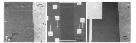
Fig.6 (a)A SEM image of crossed SWNT-SLG junctions,(b)SEM images of a representative nanodevice
2 Conclusions
In this study,we detailed a nondestructive method to mass produce crossed SWNT-SLG junctions through twice PMMA-mediated transfer techniques and selective oxygen plasma etching.SLGs used here were grown over large areas on Cu films by a CVD method.Then graphene sheet array with desired patterns were made by applying oxygen plasma etching through a shadow mask after the first transfer step.Raman and conductance measurements show that the quality and electrical properties of our SLG sheets are uniform over a large area.Finally,crossed SWNT-SLG junctions can be easily achieved by transferring the graphene sheet array onto the target substrates with well-aligned SWNT arrays.Characterization of the electrical properties of nanodevices based these heterojunctions is underway and will be reported in due time.In addition to forming crossed SWNTSLG junctions,SLG synthesis and device fabrication discussed in this article also provides a reliable method to pattern graphene sheet arrays for making graphene-based microdevices over large areas and with high yield.This technique is compatible with standard thin film technologies and allows SLG to be integrated into large scale electronics circuitry within several simple steps that can be easily streamlined and automated.These results might offer the platform for the creation of a wide variety of molecular rectifiers and other functional nano/molecular devices.
1 Aviram,A.;Ratner,M.A.Chem.Phys.Lett.,1974,29:277
2 Martin,A.S.;Sambles,J.R.;Ashwell,G.J.Phys.Rev.Lett.,1993, 70:218
3 Zhou,S.Q.;Liu,Y.Q.;Qiu,W.F.;Xu,Y.;Huang,X.B.;Li,Y.S.; Jiang,L.;Zhu,D.B.Adv.Funct.Mater.,2002,12:65
4 Chabinyc,M.L.;Chen,X.X.;Holmlin,R.E.;Jacobs,H.; Skulason,H.;Frisbie,C.D.;Mujica,V.;Ratner,M.A.;Rampi,M. A.;Whitesides,G.M.J.Am.Chem.Soc.,2002,124:11730
5 Elbing,M.;Ochs,R.;Koentopp,M.;Fischer,M.;von Hanisch,C.; Weigend,F.;Evers,F.;Weber,H.B.;Mayor,M.Proc.Natl.Acad. Sci.U.S.A.,2005,102:8815
6 Metzger,R.M.Chem.Rev.,2003,103:3803
7 Hochbaum,A.I.;Yang,P.D.Chem.Rev.,2010,110:527
8 Hu,J.T.;Ouyang,M.;Yang,P.D.;Lieber,C.M.Nature,1999, 399:48
9 Zhang,Y.;Ichihashi,T.;Landree,E.;Nihey,F.;Iijima,S.Science, 1999,285:1719
10 Meng,G.W.;Han,F.M.;Zhao,X.L.;Chen,B.S.;Yang,D.C.; Liu,J.X.;Xu,Q.L.;Kong,M.G.;Zhu,X.G.;Jung,Y.J.;Yang, Y.J.;Chu,Z.Q.;Ye,M.;Kar,S.;Vajtai,R.;Ajayan,P.M.Angew. Chem.Int.Edit.,2009,48:7166
11 Asaka,K.;Nakahara,H.;Saito,Y.Appl.Phys.Lett.,2008,92: 023114
12 Luo,J.;Zhang,L.;Zhang,Y.J.;Zhu,J.Adv.Mater.,2002,14: 1413
13 Rodriguez-Manzo,J.A.;Banhart,F.;Terrones,M.;Terrones,H.; Grobert,N.;Ajayan,P.M.;Sumpter,B.G.;Meunier,V.;Wang, M.;Bando,Y.;Golberg,D.Proc.Natl.Acad.Sci.U.S.A.,2009, 106:4591
14 Xiao,S.X.;Tang,J.Y.;Beetz,T.;Guo,X.F.;Tremblay,N.; Siegrist,T.;Zhu,Y.M.;Steigerwald,M.;Nuckolls,C.J.Am. Chem.Soc.,2006,128:10700
15 Jiao,L.Y.;Fan,B.;Xian,X.J.;Wu,Z.Y.;Zhang,J.;Liu,Z.F. J.Am.Chem.Soc.,2008,130:12612
16 Iijima,S.Nature,1991,354:56
17 Novoselov,K.S.;Geim,A.K.;Morozov,S.V.;Jiang,D.;Zhang, Y.;Dubonos,S.V.;Grigorieva,I.V.;Firsov,A.A.Science,2004, 306:666
18 Feldman,A.K.;Steigerwald,M.L.;Guo,X.;Nuckolls,C.Acc. Chem.Res.,2008,41:1731
19 Dai,H.Acc.Chem.Res.,2002,35:1035
20 Guo,X.;Nuckolls,C.J.Mater.Chem.,2009,19:5470
21 Geim,A.K.;Novoselov,K.S.Nature Mater.,2007,6:183
22 Zhang,Y.;Tan,Y.W.;Stormer,H.L.;Kim,P.Nature,2005,438: 201
23 Fuhrer,M.S.;Nygard,J.;Shih,L.;Forero,M.;Yoon,Y.G.; Mazzoni,M.S.C.;Choi,H.J.;Ihm,J.;Louie,S.G.;Zettl,A.; McEuen,P.L.Science,2000,288:494
24 Berger,C.;Song,Z.M.;Li,X.B.;Wu,X.S.;Brown,N.;Naud,C.; Mayou,D.;Li,T.B.;Hass,J.;Marchenkov,A.N.;Conrad,E.H.; First,P.N.;de Heer,W.A.Science,2006,312:1191
25 Dawlaty,J.M.;Shivaraman,S.;Chandrashekhar,M.;Rana,F.; Spencer,M.G.Appl.Phys.Lett.,2008,92:042116
26 Eda,G.;Fanchini,G.;Chhowalla,M.Nat.Nanotech.,2008,3:270
27 Dikin,D.A.;Stankovich,S.;Zimney,E.J.;Piner,R.D.;Dommett, G.H.B.;Evmenenko,G.;Nguyen,S.T.;Ruoff,R.S.Nature, 2007,448:457
28 Reina,A.;Jia,X.T.;Ho,J.;Nezich,D.;Son,H.B.;Bulovic,V.; Dresselhaus,M.S.;Kong,J.Nano Lett.,2009,9:30
29 Kim,K.S.;Zhao,Y.;Jang,H.;Lee,S.Y.;Kim,J.M.;Kim,K.S.; Ahn,J.H.;Kim,P.;Choi,J.Y.;Hong,B.H.Nature,2009,457: 706
30 Li,X.S.;Cai,W.W.;An,J.H.;Kim,S.;Nah,J.;Yang,D.X.; Piner,R.;Velamakanni,A.;Jung,I.;Tutuc,E.;Banerjee,S.K.; Colombo,L.;Ruoff,R.S.Science,2009,324:1312
31 Guo,X.;Xiao,S.;Myers,M.;Miao,Q.;Steigerwald,M.L.; Nuckolls,C.Proc.Natl.Acad.Sci.U.S.A.,2009,106:691
32 Liu,S.;Li,J.M.;Shen,Q.;Cao,Y.;Guo,X.F.;Zhang,G.M.; Teng,C.Q.;Zhang,J.;Liu,Z.F.;Steigerwald,M.L.;Xu,D.S.; Nuckolls,C.Angew.Chem.Int.Edit.,2009,48:4759
33 Dai,H.Acc.Chem.Res.,2002,35:1035
34 Liu,S.;Shen,Q.;Cao,Y.;Gan,L.;Wang,Z.;Steigerwald,M.L.; Guo,X.Coord.Chem.Rev.,2010,254:1101
猜你喜歡
中國機械工程(2022年22期)2022-11-25 08:24:30
中國機械工程(2022年7期)2022-04-20 03:25:38
雜文月刊(2019年19期)2019-12-04 07:48:34
中國機械工程(2019年17期)2019-09-19 07:43:32
中國機械工程(2018年4期)2018-03-06 05:34:58
試題與研究·教學(xué)論壇(2017年6期)2017-02-28 05:41:10
中國三峽(2016年5期)2017-01-15 13:58:43
云南師范大學(xué)學(xué)報(自然科學(xué)版)(2015年5期)2015-12-26 12:46:16
中央民族大學(xué)學(xué)報(自然科學(xué)版)(2015年2期)2015-06-09 08:45:26
現(xiàn)代企業(yè)文化(2015年1期)2015-02-28 18:58:45
